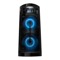
GTK-XB5
GTK-XB5
2121
For Schematic Diagrams.
Note:
• All capacitors are in μF unless otherwise noted. (p: pF) 50
WV or less are not indicated except for electrolytics and
tantalums.
• All resistors are in Ω and 1/4 W or less unless otherwise
specifi ed.
THIS NOTE IS COMMON FOR PRINTED WIRING BOARDS AND SCHEMATIC DIAGRAMS.
(In addition to this, the necessary note is printed in each block.)
For Printed Wiring Boards.
Note:
• : Pattern from the side which enables seeing.
(The other layers’ patterns are not indicated.)
• Circuit Boards Location
Caution:
Pattern face side:
(Conductor Side)
Parts face side:
(Component Side)
Parts on the pattern face side seen
from the pattern face are indicated.
Parts on the parts face side seen from
the parts face are indicated.
Note:
The components identi-
fi ed by mark 0 or dotted
line with mark 0 are criti-
cal for safety.
Replace only with part
number specifi ed.
Note:
Les composants identifi és
par une marque 0 sont
critiques pour la sécurité.
Ne les remplacer que par
une pièce portant le nu-
méro spécifi é.
POWER board
SPEAKER LED (BTM) board
SPEAKER LED (TOP) board
FLASH LED board
TUBE LED RIGHT board
CONTRL board
MAIN board
NFC board
TUBE LED LEFT board
TUBE LED board
Note: When replacing the MAIN board or the NFC board,
be sure to replace the MAIN board and the NFC board
simultaneously.
The MAIN board or the NFC board cannot replace with
single.
Among the repair parts, the MAIN board and the NFC
board are supplied as one unit.
Note: When replacing the MAIN board or the NFC board,
be sure to replace the MAIN board and the NFC board
simultaneously.
The MAIN board or the NFC board cannot replace with
single.
Among the repair parts, the MAIN board and the NFC
board are supplied as one unit.
 Loading...