Do you have a question about the Sony HCD-ECL5 and is the answer not in the manual?
Technical details of audio amplification.
Specifications for FM/AM radio reception.
Details about the CD playback mechanism.
Audio and data input specifications.
Speaker impedance and output details.
USB port specifications and capabilities.
List of compatible audio file types.
General unit specifications like power and dimensions.
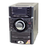
Information on identifying the unit's model number.
Precautions for handling sensitive optical components.
Safety and procedure for checking laser emission.
Information and handling of lead-free solder.
Guidance on replacing specific board components.
Recommended discs for operational checks.
Procedure to unlock the CD tray.
Safety procedure for discharging capacitors.
Overview of the unit's disassembly sequence.
Steps to remove the outer covers.
Procedure for removing the rear panel and power cord.
Steps to remove the CD door mechanism.
Procedure to detach the front panel assembly.
Steps to remove the main board assembly.
Detailed steps for main board removal.
Procedure for removing the power supply board.
Steps to remove the front panel control board.
Procedure to remove the USB interface board.
Steps for removing the CD loader mechanism.
How to check the unit's firmware version.
Procedure to restore factory default settings.
How to enable and disable the disc tray lock function.
Instructions for activating and deactivating the child lock feature.
Procedure to test the fluorescent indicator tube display.
Procedures for checking the CD playback circuitry.
Method for verifying the RF signal waveform for CD playback.
Overall system block diagram for understanding data flow.
Component layout for the main circuit board.
Electrical schematic for power input and regulators.
Electrical schematic for MPEG decoder and memory interface.
Electrical schematic for USB port and power switching.
Electrical schematic for RTC, VFD, and MCU interfaces.
Electrical schematic for FM tuner input and audio switching.
Electrical schematic for audio processor and amplifier control.
Electrical schematic for the power amplifier stages.
Component layout for tuner and USB boards.
Electrical schematics for tuner and USB circuitry.
Component layout for the front panel control board.
Electrical schematic for front panel controls and display.
Electrical schematic for the power supply unit.
Component layout for the power supply board.
Exploded view and parts list for external covers.
Exploded view and parts list for the rear panel assembly.
Exploded view and parts list for the front panel components.
Exploded view and parts list for internal main assemblies.
| Brand | Sony |
|---|---|
| Model | HCD-ECL5 |
| Category | Car Receiver |
| Preset Stations | 30 |
| USB Port | Yes |
| Audio Line In | Yes |
| Bluetooth | No |
| Functions | CD player |
| Supported Media | CD-R, CD-RW |
| Tuner Bands | FM, AM |