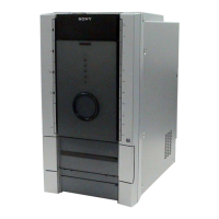
94
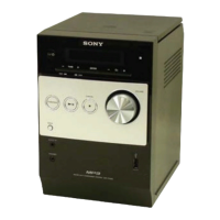
HCD-FLX5D/FLX7D
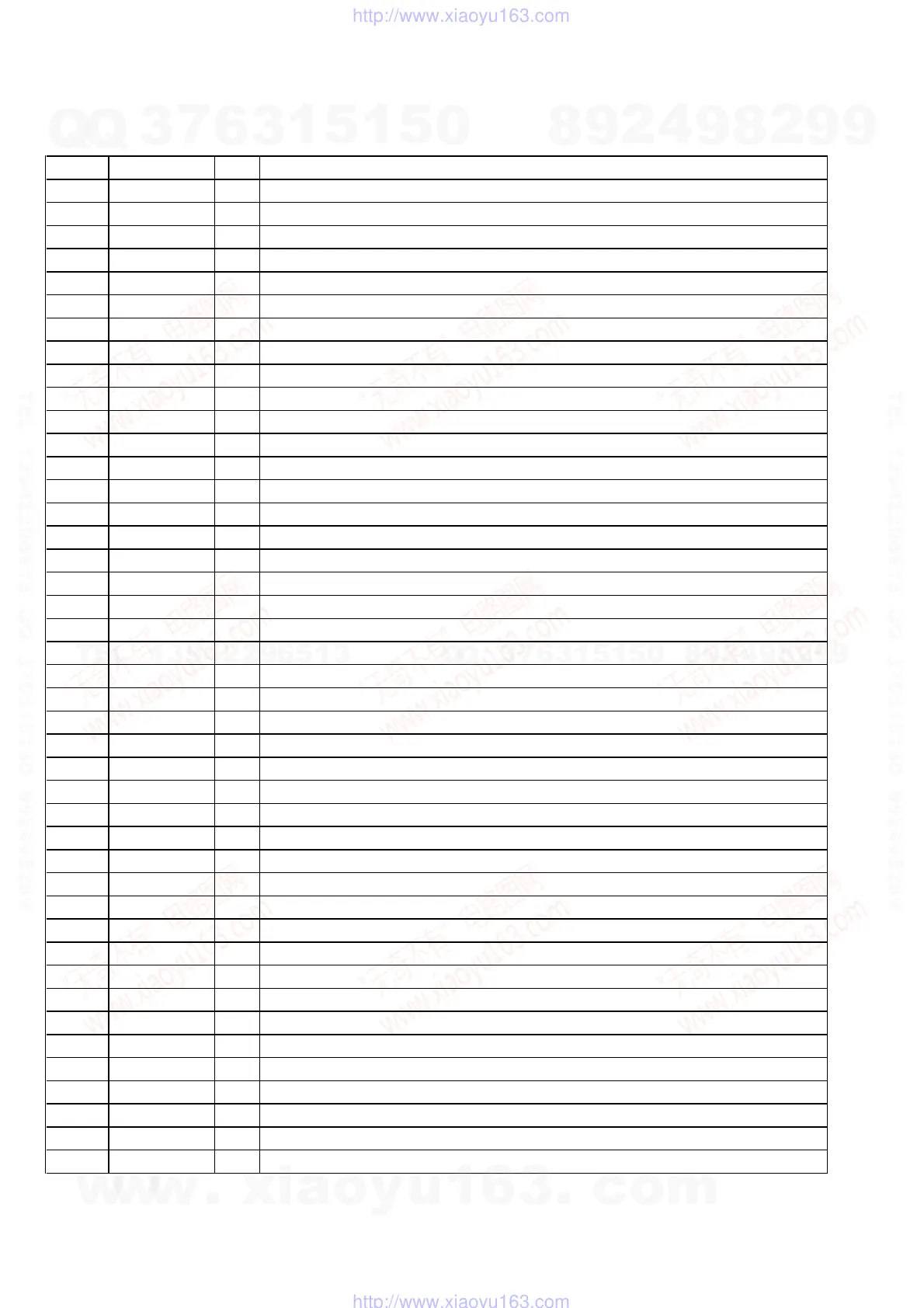
MB BOARD IC206 ZIVA5X-C2F (DVD SYSTEM PROCESSOR)
Pin No. Pin Name I/O Description
1 VDDP — Power supply terminal (+3.3V)
2 HA1 O Address signal output to the program ROM and bus interface
3 to 11 HAD15 to HAD7 I/O Two-way data bus with the program ROM and bus interface
12 VDDP — Power supply terminal (+3.3V)
13 GNDP — Ground terminal
14 to 19 HAD6 to HAD1 I/O Two-way data bus with the program ROM and bus interface
20 VDDP — Power supply terminal (+3.3V)
21 GNDP — Ground terminal
22 HAD0 I/O Two-way data bus with the program ROM and bus interface
23 HDTACK I Acknowledge signal input terminal for host data transfer Not used
24 HIRQ0 I Interrupt signal input terminal Not used
25 WEH.UDS O Write enable host upper data strobe signal output to the program ROM
26 WEL.LDS O Write enable host lower data strobe signal output terminal Not used
27 HREAD O Output enable signal output to the program ROM
28 GPIO0 (1) I Check jig detection signal input terminal
29 GND — Ground terminal
30 VDD — Power supply terminal (+1.8V)
31 GND25 — Ground terminal
32 VDD25 — Power supply terminal (+3.3V)
33 to 42 MA9 to MA0 O Address signal output to the SD-RAM
43 GND25 — Ground terminal
44 VDD25 — Power supply terminal (+3.3V)
45, 46 MA10, MA11 O Address signal output to the SD-RAM
47, 48 BA1, BA0 O Bank select signal output to the SD-RAM
49 MCS0 O Chip select signal output to the SD-RAM
50 MCS1 O Chip select signal output terminal Not used
51 MRAS O Row address strobe signal output to the SD-RAM
52 MCAS O Column address strobe signal output to the SD-RAM
53 MWE O Write enable signal output to the SD-RAM
54 GND25 — Ground terminal
55 VDD25 — Power supply terminal (+3.3V)
56 MCLK O Clock signal output to the SD-RAM
57 to 60 MD0 to MD3 I/O Two-way data bus with the SD-RAM
61 GND25 — Ground terminal
62 MDQM0 O Write mask signal output to the SD-RAM
63 VDD25 — Power supply terminal (+3.3V)
64 to 71 MD4 to MD11 I/O Two-way data bus with the SD-RAM
72 GND25 — Ground terminal
73 MDQM1 O Write mask signal output to the SD-RAM
74 VDD25 — Power supply terminal (+3.3V)
75 to 78 MD12 to MD15 I/O Two-way data bus with the SD-RAM
79 GND — Ground terminal
80 VDD — Power supply terminal (+1.8V)
• IC Pin Function Description
w
w
w
.
x
i
a
o
y
u
1
6
3
.
c
o
m
Q
Q
3
7
6
3
1
5
1
5
0
9
9
2
8
9
4
2
9
8
T
E
L
1
3
9
4
2
2
9
6
5
1
3
9
9
2
8
9
4
2
9
8
0
5
1
5
1
3
6
7
3
Q
Q
TEL 13942296513 QQ 376315150 892498299
TEL 13942296513 QQ 376315150 892498299
http://www.xiaoyu163.com
http://www.xiaoyu163.com