54
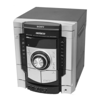
HCD-GNX60/GNX70/GX9900
Pin No. Pin Name I/O Description
50 SW LED2 O Not used (Open)
51 B-PLAY I Deck B playback detection signal input
52 THERMAL VACS I Thermal VACS detection input
53 A-TRIG O Deck A side trigger plunger drive signal output
54 CAPM-CONT O Capstan motor drive signal output
55 B-TRIG O Deck B side trigger plunger drive signal output
56 REC BIAS O Recording bias on/off control signal output
57 TC-RELAY O Recording/playback selection signal output
58 ALC O Automatic limiter control signal output
59 PB-AB O Deck A/B playback selection signal output
60 AMS-IN I Not used.
61 UNDER VOLTAGE DET I Under-voltage protection detection input
62 VCC — Power supply(+3.3V)
63 OVER VOLTAGE I Over-voltage protection detection input
64 VSS — Ground
65 TC MUTE O Tape playback muting on/off signal output
66 LINE MUTE O Line muting on/off signal output
67 REC MUTE O Recording muting on/off signal output
68 SW RY O Not used (Open)
69 STBY-RLY O Main power on/off signal output
70 PROT I Speaker protect detection signal input
71 GC-RESET O GC reset signal output
72 STBY-LED/FAN CTRL O POWER indicator LED drive signal output
73 DISPLAY-KEY I DISPLAY key press detection Interrupt signal input
74 POWER-KEY I POWER key press detection Interrupt signal input
75 HP-MUTE O Headphone muting on/off signal output
76 FR RELAY O front speakers relay drive signal output
77 LINK/SURR-RLY O Surround speaker mode control signal output
78 STK-MUTE O Power amplifier and sub woofer amplifier on/off control signal output
79 M61530-DATA O Not used (Open)
80 M61530-CLK O Not used (Open)
81 M61529-DATA O Serial data output to M61529FP
82 M61529-CLK O Serial transfer clock signal output to M61529FP
83 SW ON LED O Not used (Open)
84 ST-CE O PLL chip enable signal output to the tuner unit
85 MC DIN (ST) O PLL serial data output to the tuner unit
86 ST-CLK I PLL serial transfer clock signal output to the tuner unit
87 MC DOUT (ST) I PLL serial data input from the tuner unit
88 TUNED I Tuning detection signal input from the tuner unit
89 A SHUT I Shut off detection signal input from deck A side reel pulse detector
90 B SHUT I Shut off detection signal input from deck A side reel pulse detector
91 SW AD KEY I Not used (pull up)
92 MODEL-IN I Model input
93 DEST-IN I Destination input
94 B-HALF I
Deck B cassette , forward side recording tab and reverse side recording tab detection signal input
95 SW VOL IN I Subwoofer on/off signal input
96 AVSS — Ground
97 BPF DET I Low frequency signal input from NJM2760 for RANDOM mode
98 VREF I A/D reference voltage input
99 AVCC — Power supply (+3.3V)
100 HP DET I Headphone connection detection signal input
 Loading...