76
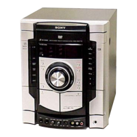
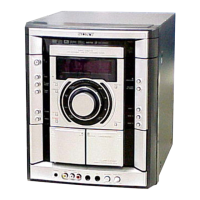
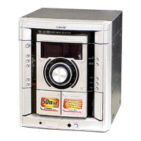
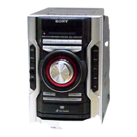
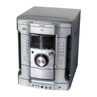
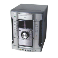
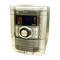
HCD-GNZ77D/GNZ88D
Pin No. Pin Name I/O Pin Description
47 TM R O CDM turning motor control signal output
48 LM F O CDM loading motor control signal output
49 LM R O CDM loading motor control signal output
50 LED ILLUMINATION 1 O
Dynamic LED drive signal output to the ILLUMINATION 1st indicator and
2nd indicator “H”: LED on
51 LED ILLUMINATION 2 O
Dynamic LED drive signal output to the ILLUMINATION 3rd indicator and
4th indicator “H”: LED on
52 LED ILLUMINATION 3 O
Dynamic LED drive signal output to the ILLUMINATION 5th indicator and
6th indicator “H”: LED on
53 LED CTRL O Dynamic LED drive select signal output
54 VOL A I Jog dial pulse input from the VOLUME rotary encoder (A phase input)
55 VOL B I Jog dial pulse input from the VOLUME rotary encoder (B phase input)
56 STBY LED O LED drive signal output of POWER indicator “H”: LED is turned on
57 FL DRIVER DATA O Serial data output signal to FL Driver, NJU3427
58 FL DRIVER CLK O Serial data clock signal to FL Driver, NJU3427
59 FL DRIVER RESET O Serial data reset signal to FL Driver, NJU3427
60 FL DRIVER CS O Serial data chip select signal to FL Driver, NJU3427
61 SW LED O LED drive signal output of SUB WOOFER ON indicator “H”: LED ON
62 VCC — Power supply pin (+3.3 V)
63 A HALF I Deck A cassette detection signal input “H”: cassette detected
64 VSS — Ground pin
65 SM RESET O Reset signal output to the S-Master Power IC
66 IO EXP DATA OUT O Serial data output signal to I/O expander, BH2210V
67 NO USE I Not used. (Connect to ground.)
68 IO EXP RST O Reset signal output to the I/O expander, BH2210V
69 IO EXP CLK O Serial data latch signal to I/O expander, BH2210V
70 IO EXP LAT O Serial data clock signal to I/O expander, BH2210V
71 NO USE I Not used. (Connect to ground.)
72 SM SD I Shutdown (protector) detection signal from the S-Master power IC
73 DISPLAY KEY I DISPLAY key press detection signal (Interrupt input)
74 POWER KEY I POWER key press detection signal (Interrupt input)
75 NO USE I Not used. (Connect to ground.)
76 SM LATCH 1 O Serial data latch pulse output to the S-Master Processor
77 SM CLK O Serial data transfer clock signal to the S-Master Processor IC (CXD9843)
78 SM DATA O Serial data output signal to the S-Master Processor IC (CXD9843)
79 SM LATCH 2 O Serial data latch pulse output to the S-Master Processor
80 NO USE I Not used. (Connect to ground.)
81 NO USE/SW MUTE O GNZ88D: Not used. (Connect to ground.), GNZ77D: Subwoofer mute signal output
82 OUT2DLY SEL I PWM Mode selection signal “L”: PWM Mode 3, “H”: PWM Mode 4
83 M61537 DATA O Serial data output to audio signal processor, M61537FP
84 M61537 CLK O Serial data transfer clock signal output to audio signal processor, M61537FP
85 HP DET I Headphone connection detection signal input “H”: headphone connected
86 HP MUTE O Headphone muting on/off control signal “H”: muting on
87 NO USE I Not used. (Connect to ground.)
88 VACS IN I VACS level detection signal
89 A SHUT I Shut off detection signal input from deck A side reel pulse detector (A/D input)
90 B SHUT I Shut off detection signal input from deck B side reel pulse detector (A/D input)
91 B HALF I
Deck B cassette detection and forward side recording tab detection signal input
(A/D input)
92 MODEL IN I Model setting (A/D input)
93 DEST IN I Destination setting (A/D input)
94 AD KEY 3 I Key signal input (A/D input)
95 AD KEY 2 I Key signal input (A/D input)
w
w
w
.
x
i
a
o
y
u
1
6
3
.
c
o
m
Q
Q
3
7
6
3
1
5
1
5
0
9
9
2
8
9
4
2
9
8
T
E
L
1
3
9
4
2
2
9
6
5
1
3
9
9
2
8
9
4
2
9
8
0
5
1
5
1
3
6
7
3
Q
Q
TEL 13942296513 QQ 376315150 892498299
TEL 13942296513 QQ 376315150 892498299
http://www.xiaoyu163.com
http://www.xiaoyu163.com