EasyManua.ls Logo

Sony HCD-GNZ8D User Manual

Sony HCD-GNZ8D
108 pages
To Next Page IconTo Next Page
Page #1 background imageLoading...
Page #1 background image
1
Ver. 1.1 2005. 12
Model Name Using Similar Mechanism NEW
DVD
DVD Mechanism Type CDM74HF-DVBU101//C
Section
Optical Pick-up Name KHM-310CAB/C2NP
Tape Deck
Model Name Using Similar Machanism NEW
Section
SERVICE MANUAL
E Model
HCD-GNZ7D/GNZ8D/GNZ9D
Australian Model
HCD-GNZ9D
HCD-GNZ7D/GNZ8D/GNZ9D
Amplifier section
HCD-GNZ9D
The following measured at AC 120, 127, 220, 230 – 240 V,
50/60 Hz
Continuous RMS power output (reference)
Front speaker: 115 + 115 watts
(6 ohms at 1 kHz, 10%
THD)
Center speaker: 50 watts (6 ohms at 1 kHz,
10% THD)
Surround speaker: 50 + 50 watts
(6 ohms at 1 kHz, 10%
THD)
Subwoofer: 170 watts (4 ohms at
100 Hz, 10% THD)
HCD-GNZ8D
The following measured at AC 120, 127, 220, 230 – 240 V,
50/60 Hz
Continuous RMS power output (reference)
Front speaker: 100 + 100 watts
(6 ohms at 1 kHz, 10%
THD)
Center speaker: 40 watts (6 ohms at 1 kHz,
10% THD)
Surround speaker: 40 + 40 watts
(6 ohms at 1 kHz, 10%
THD)
HCD-GNZ7D
The following measured at AC 120, 127, 220, 230 – 240 V,
50/60 Hz
Continuous RMS power output (reference)
100 + 100 watts
(6 ohms at 1 kHz, 10%
THD)
SPECIFICATIONS
Inputs
VIDEO/SAT IN (audio) (phono jacks):
voltage 450/250 mV,
impedance 47 kilohms
VIDEO INPUT VIDEO (phono jack):
1 Vp-p, 75 ohms
VIDEO INPUT AUDIO (phono jacks):
voltage 250 mV,
impedance 47 kilohms
MIC1/MIC2 (phone jack):
sensitivity 1 mV,
impedance 10 kilohms
Outputs
VIDEO/SAT OUT (audio) (phono jacks):
voltage 250 mV,
impedance 1 kilohm
VIDEO OUT (phono jack):
max. output level
1 Vp-p, unbalanced, Sync
negative, load impedance
75 ohms
S-VIDEO OUT (4-pin/mini-DIN jack):
Y: 1 Vp-p, unbalanced,
Sync negative,
C: 0.286 Vp-p, load
impedance 75 ohms
COMPONENT VIDEO OUT:
Y: 1 Vp-p, 75 ohms
PB, PR: 0.7 Vp-p, 75 ohms
Sony Corporation
Home Audio Division
Published by Sony Engineering Corporation
9-879-622-02
2005L04-1
© 2005. 12
– Continued on next page –
DVD DECK RECEIVER
(Photo: HCD-GNZ7D)
HCD-GNZ7D/GNZ8D/GNZ9D are
the tuner, deck, DVD and amplifier
section in MHC-GNZ7D/GNZ8D/
GNZ9D.
w
w
w
.
x
i
a
o
y
u
1
6
3
.
c
o
m
Q
Q
3
7
6
3
1
5
1
5
0
9
9
2
8
9
4
2
9
8
T
E
L
1
3
9
4
2
2
9
6
5
1
3
9
9
2
8
9
4
2
9
8
0
5
1
5
1
3
6
7
3
Q
Q
TEL 13942296513 QQ 376315150 892498299
http://www.xiaoyu163.com

Table of Contents

Question and Answer IconNeed help?

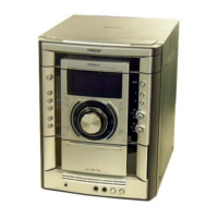
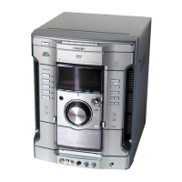
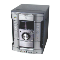
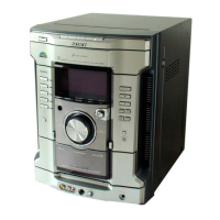
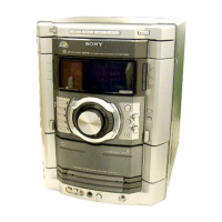
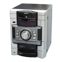
Do you have a question about the Sony HCD-GNZ8D and is the answer not in the manual?

Sony HCD-GNZ8D Specifications

General IconGeneral
BrandSony
ModelHCD-GNZ8D
CategoryStereo System
LanguageEnglish

Summary

Safety and Handling Precautions

Laser Diode Emission Check

Safety measures for laser diode emission checks.

Section 3 Disassembly

Disassembly Flowchart

Visual guide for unit disassembly sequence.

Section 4 Test Mode

Basic Test Procedures

Covers Cold Reset, Tuner, TV/SAT, Color System, Disc Tray Lock.

Common Test Mode and Ship Modes

Tests amplifier, tape, and ship modes.

DVD Section Test Mode

Mirror Time Adjustment

Procedure for adjusting mirror time.

IOP Measurement

Procedure for executing IOP measurement.

Drive Manual Operation

Sub-menu for manual drive operations.

Section 5 Mechanical Adjustments

Precautions and Torque Measurement

General precautions and torque specifications.

Section 6 Electrical Adjustments

DVD and Deck Section Adjustments

Covers DVD level checks and deck azimuth adjustment.

7-5. Block Diagram - Function/Power Section

Power Supply Diagram

Shows the power supply block and its connections.

7-6. Printed Wiring Boards - Driver Section

Driver Section Board Layouts

Printed wiring boards for Driver section components.

7-7. Schematic Diagram - Driver Section

Driver Section Schematic

Circuit diagram for the driver section.

7-8. Printed Wiring Board - DMB10 Section (Side A)

DMB10 Board (Side A) Layout

Component layout for DMB10 board, Side A.

7-9. Printed Wiring Board - DMB10 Section (Side B)

DMB10 Board (Side B) Layout

Component layout for DMB10 board, Side B.

7-10. Schematic Diagram - DMB10 Section (1/4)

DMB10 Schematic Part 1

First part of the DMB10 schematic diagram.

7-11. Schematic Diagram - DMB10 Section (2/4)

DMB10 Schematic Part 2

Second part of the DMB10 schematic diagram.

7-12. Schematic Diagram - DMB10 Section (3/4)

DMB10 Schematic Part 3

Third part of the DMB10 schematic diagram.

7-13. Schematic Diagram - DMB10 Section (4/4)

DMB10 Schematic Part 4

Fourth part of the DMB10 schematic diagram.

7-14. Printed Wiring Board - Audio Section

Audio Section Board Layout

Component layout for the Audio section.

7-15. Schematic Diagram - Audio Section (1/3)

Audio Section Schematic Part 1

First part of the Audio section schematic.

7-16. Schematic Diagram - Audio Section (2/3)

Audio Section Schematic Part 2

Second part of the Audio section schematic.

7-17. Schematic Diagram - Audio Section (3/3)

Audio Section Schematic Part 3

Third part of the Audio section schematic.

7-18. Printed Wiring Board - Video Section

Video Section Board Layout

Component layout for the Video section.

7-19. Schematic Diagram - Video Section

7-20. Printed Wiring Board - Front AMP Section

7-21. Schematic Diagram - Front AMP Section

7-22. Printed Wiring Boards - Panel Section

7-23. Schematic Diagram - Panel Section (1/2)

7-24. Schematic Diagram - Panel Section (2/2)

7-25. Printed Wiring Board - Jack Section

7-26. Schematic Diagram - Jack Section

7-27. Printed Wiring Board - Surround AMP Section (HCD-GNZ8D/GNZ9D)

7-28. Schematic Diagram - Surround AMP Section (HCD-GNZ8D/GNZ9D)

7-29. Printed Wiring Board - Subwoofer Section (HCD-GNZ9D)

7-30. Schematic Diagram - Subwoofer Section (HCD-GNZ9D)

7-31. Printed Wiring Board - Trans Section

7-32. Printed Wiring Board - Sub Trans Section

7-33. Schematic Diagram - Power Section

Section 8 Exploded Views

8-7. Audio Board Section

8-8. DVD Mechanism Deck Section (1)

8-9. DVD Mechanism Deck Section (2)

Service Manual Supplement-1

Subject: Board Change to DMB11

Information on board change from DMB10 to DMB11.

How to Distinguish Boards

Printed Wiring Board - DMB11 Section (Side A)

Printed Wiring Board - DMB11 Section (Side B)

Related product manuals