EasyManua.ls Logo

Sony HCD-GN77D User Manual

Sony HCD-GN77D
114 pages
To Next Page IconTo Next Page
Page #1 background imageLoading...
Page #1 background image
SERVICE MANUAL
Model Name Using Similar Mechanism NEW
DVD
DVD Mechanism Type CDM74D-DVBU23
Section
Base Unit Name DVBU23
Optical Pick-up Name TDP022W
Tape Model Name Using Similar Mechanism HCD-GN800
Section Tape Transport Mechanism Type CWM43RR23
MiNi Hi-Fi COMPONENT SYSTEM
E Model
HCD-GN77D
Ver 1.1 2003.08
9-877-454-02 Sony Corporation
2003H02-1 Home Audio Company
C 2003.08 Published by Sony Engineering Corporation
SPECIFICATIONS
HCD-GN77D is the amplifier, DVD
player, tape deck and tuner section in
MHC-GN77D.
– Continued on next page –
Amplifier section
The following are measured at AC 120, 127, 220, 240V 50/60 Hz
DIN power output (rated)
Front speaker: 110 + 110 watts (6 ohms at 1 kHz, DIN)
Center speaker: 30 watts (8 ohms at 1 kHz, DIN)
Surround speaker: 30 + 30 watts (8 ohms at 1 kHz, DIN)
Continuous RMS power output (reference)
Front speaker: 150 + 150 watts (6 ohms at 1 kHz, 10% THD)
Center speaker: 40 watts (8 ohms at 1 kHz, 10% THD)
Surround speaker: 40 + 40 watts (8 ohms at 1 kHz, 10% THD)
Inputs
GAME (VIDEO): 1 Vp-p, 75 ohms (phono jack)
GAME (AUDIO): Voltage 250 mV,
(phono jacks) impedance 47 kilohms
MD/VIDEO (AUDIO) IN: voltage 450 mV/250 mV,
(phono jacks) impedance 47 kilohms
MIC: sensitivity 1 mV,
(phone jack) impedance 10 kilohms
Outputs
AUDIO OUT: Voltage 250 mV
(phono jacks) impedance 1 kilohms
VIDEO OUT: max. output level 1 Vp-p,
(phono jack) unbalanced, Sync.
negative load impedance 75 ohms
COMPONENT VIDEO
OUT: Y: 1 Vp-p, 75 ohms
PB/CB: 0.7 Vp-p, 75 ohms
PB/CR: 0.7 Vp-p, 75 ohms
S VIDEO OUT
(4-pin/mini-DIN jack): Y: 1 Vp-p, unbalanced, Sync negative
C: 0.286 Vp-p load impedance 75 ohms
PHONES: accepts headphones of 8 ohms or more
(stereo mini jack)
FRONT SPEAKER: accepts impedance of 6 to 16 ohms
SUBWOOFER OUT: Voltage 250 mV
(phono jack) impedance 1 kilohms
SURROUND SPEAKER: accepts impedance of 8 ohms to 16 ohms
CENTER SPEAKER: accept impedance of 8 ohms to 16 ohms
Disc player section
Laser Semiconductor laser
(DVD: λ = 650 nm, CD: λ = 780 nm)
Emission duration: continuous
Frequency response DVD (PCM 48 kHz): 2 Hz – 22 kHz = (±1dB)
CD: 2 Hz – 20 kHz (±0.5 dB)
Video color system format NTSC, PAL
(except Latin American models)
DVD DIGITAL OUT (OPTICAL)
(Square optical connector jack, rear panel)
Wave length 660 nm
w
w
w
.
x
i
a
o
y
u
1
6
3
.
c
o
m
Q
Q
3
7
6
3
1
5
1
5
0
9
9
2
8
9
4
2
9
8
T
E
L
1
3
9
4
2
2
9
6
5
1
3
9
9
2
8
9
4
2
9
8
0
5
1
5
1
3
6
7
3
Q
Q
TEL 13942296513 QQ 376315150 892498299
http://www.xiaoyu163.com

Table of Contents

Question and Answer IconNeed help?

Do you have a question about the Sony HCD-GN77D and is the answer not in the manual?

Sony HCD-GN77D Specifications

General IconGeneral
BrandSony
ModelHCD-GN77D
CategoryStereo System
LanguageEnglish

Summary

SERVICE MANUAL

HCD-GN77D Model Information

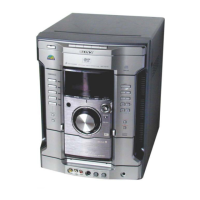
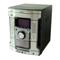
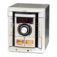
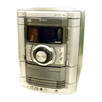
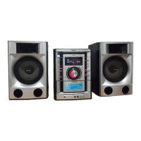
Model identifier for the Hi-Fi component system.

System Specifications

Technical specifications for Amplifier and Disc Player sections.

Model Specifications and Notes

Tape and Tuner Sections

Specifications for the cassette tape and tuner sections.

General Specifications

General specifications including power, dimensions, and mass.

Unleaded Solder Precautions

Information and precautions regarding the use of unleaded solder.

Servicing Notes

Optical Pick-up and Laser Diode Handling

Handling precautions for optical pick-up and laser diode checks.

Model Identification and Tray Lock

Model variants and procedure for DVD tray lock mode.

General Information and Controls

Main Unit Controls

Alphabetical index of main unit controls and their locations.

Manual Symbols

Explanation of symbols used in the manual for controls.

Remote Control Functions

Remote Control Alphabetical Order

Alphabetical listing of remote control functions and button assignments.

Remote Control Symbols

Explanation of symbols used on the remote control.

Disassembly Procedure

Disassembly Sequence Overview

Flowchart illustrating the recommended disassembly sequence of the unit.

Disassembly: Case and Loading Panel

3-1. Case Disassembly

Procedure for disassembling the unit's case.

3-2. Loading Panel Disassembly

Procedure for disassembling the disc loading mechanism or panel.

Disassembly: Front Panel and Tuner Pack

3-3. Front Panel Assy Disassembly

Procedure for disassembling the front panel assembly.

3-4. Tuner Pack and Sub Trans Board Disassembly

Procedure for disassembling the tuner pack and sub trans board.

Disassembly: DVD Mechanism and Game Board

3-5. DVD Mechanism Deck Disassembly

Procedure for disassembling the DVD mechanism deck.

3-6. Game In Board and Tape Mechanism Deck Disassembly

Procedure for disassembling the game in board and tape mechanism deck.

Disassembly: CD Switch Board and Volume Board

3-7. CD Switch Board and Display Board Disassembly

Procedure for disassembling CD Switch and Display boards.

3-8. Volume Board Disassembly

Procedure for disassembling the volume control board.

Disassembly: Back Panel and Main Board

3-9. Back Panel and Subwoofer Board Disassembly

Procedure for disassembling the back panel and subwoofer board.

3-10. Main Board Disassembly

Procedure for disassembling the main circuit board.

Disassembly: Power Amp and Video Boards

3-11. Power Amp Board Disassembly

Procedure for disassembling the power amplifier board.

3-12. Video, DMB03, Regulator Board Disassembly

Procedure for disassembling video, DMB03, and regulator boards.

Disassembly: SW Board and RF Board

3-13. SW Board and Driver Board Disassembly

Procedure for disassembling SW and Driver boards.

3-14. RF Board and Pick-up Unit Disassembly

Procedure for disassembling the RF board and pick-up unit.

Disassembly: Sensor and Motor Boards

3-15. Sensor Board Disassembly

Procedure for disassembling the sensor board.

3-16. Motor (TB) Board Disassembly

Procedure for disassembling the motor (TB) board.

Disassembly: Motor (LD) Board

3-17. Motor (LD) Board Disassembly

Procedure for disassembling the motor (LD) board.

Test Mode Operations

General Control (GC) Test Mode

Procedure to enter and use the General Control (GC) test mode.

Mechanism Control (MC) Test Mode

Procedure to enter and use the Mechanism Control (MC) test mode.

Test Mode Functions

Cold Reset, VACS ON/OFF, Tuner Step, DVD Repeat Modes

Cold reset, VACS control, tuner step change, and DVD repeat limit.

DVD Ship Modes, Power Management, Tray Lock, MD/Video Switching

DVD shipping modes, power management, tray lock, and MD/Video switching.

Adjustments and Diagrams

Section 5: Mechanical Adjustments

Precautions and torque measurements for mechanical adjustments.

Section 6: Electrical Adjustments

Electrical adjustments for deck section and head azimuth.

Tape Speed Adjustment

Playback Head Adjustment

Adjusting playback head output peaks for L-CH and R-CH.

Deck B Tape Speed Adjustment

Adjusting tape speed for Deck B using a test tape.

Tape Recording Adjustments

REC BIAS ADJUSTMENT DECK B

Procedure for adjusting recording bias for Deck B.

REC LEVEL ADJUSTMENT DECK B

Procedure for adjusting the record level for Deck B.

Video Section Adjustments

Re-adjustment of Servo Circuit

Procedure for re-adjusting the servo circuit when parts are replaced.

Video Level Check (VIDEO BOARD)

Procedure to check and adjust video signal level according to NTSC standard.

Diagrams and Notes

Note on Schematic Diagram

Notes and abbreviations used in schematic diagrams.

Note on Printed Wiring Boards

Notes and abbreviations used in printed wiring boards.

Abbreviation

List of abbreviations used in the manual.

Circuit Board Locations

Component Board Locations

Identifies the physical locations of various circuit boards within the unit.

Waveform Analysis

Main Board Waveforms

Waveforms observed on the Main board.

DMB03 Board Waveforms

Waveforms observed on the DMB03 board.

Display Board Waveforms

Waveforms observed on the Display board.

RF Board Waveforms

Waveforms observed on the RF board.

Block Diagram: DVD DSP (1/2)

Optical Pick-up Block Diagram

Block diagram of the optical pick-up.

Block Diagram: DVD DSP (2/2)

DVD System Processor Block Diagram

Block diagram of the DVD System Processor IC207.

Address Latch Block Diagram

Block diagram of the Address Latch IC216.

SDRAM Block Diagram

Block diagram of the SDRAM IC203.

DVD DSP (1/2) Section Link

Link to Part 1 of the DVD DSP block diagram.

DVD DSP (2/2) Section Link

Link to Part 2 of the DVD DSP block diagram.

Main Section Link

Link to the Main Section block diagram.

Block Diagram: Tuner/Tape Deck Section

Tuner/Tape Deck Signal Paths

Signal paths for tuner and tape deck sections.

Tuner/Tape Deck Block Diagram

Overall block diagram of the tuner and tape deck sections.

Block Diagram: Main Section

Volume Control, CPU Interface, Input Select

Block diagrams for volume control, CPU interface, and input selection.

Surround Buffer, System Control, Section Links

Block diagrams for surround buffer, system control, and section links.

Block Diagram: AMP Section

Power Amplifier Blocks

Block diagrams of the power amplifier stages.

System Control and Protection Circuits

Block diagrams for system control and protection circuits.

Block Diagram: Display Section

Fluorescent Indicator Tube and Rotary Encoder

Diagrams for fluorescent tube and rotary encoder connections.

Section Links

Links to other section block diagrams (Main, DVD DSP, AMP).

Printed Wiring Board: RF Board

RF Board Layout (Side A)

Printed wiring board layout for the RF board (Side A).

RF Board Layout (Side B)

Printed wiring board layout for the RF board (Side B).

Semiconductor Location

Table listing semiconductor component locations on the RF board.

Schematic Diagram: RF Board

DVD/CD RF Amplifier Schematic

Schematic of the DVD/CD RF amplifier IC001.

Connection to DMB03 Board

Shows connections to the DMB03 board.

Printed Wiring Boards: DVD Mechanism

Motor (LD) Board Layout

Printed wiring board layout for the Motor (LD) board.

Driver Board Layout

Printed wiring board layout for the Driver board.

Sensor Board Layout

Printed wiring board layout for the Sensor board.

SW Board Layout

Printed wiring board layout for the SW board.

Semiconductor Location

Table listing semiconductor component locations.

Schematic Diagrams: DVD Mechanism

Driver Board Schematic

Schematic diagram of the Driver board.

Sensor Board Schematic

Schematic diagram of the Sensor board.

Motor (TB) Board Schematic

Schematic diagram of the Motor (TB) board.

SW Board Schematic

Schematic diagram of the SW board.

Main Board (4/4) Link

Link to Main board schematic section (4/4).

Printed Wiring Boards: DMB03 Board (Side A)

Board Links

Links to Main, Regulator, Video, and RF boards.

Semiconductor Location Table

Table listing semiconductor component locations on the DMB03 board.

Printed Wiring Boards: DMB03 Board (Side B)

IC Component Locations

Identifies locations of key IC components on the DMB03 board.

Schematic Diagram: DMB03 Board (1/8)

DMB03 Board (2/8) Link

Link to the next part of the DMB03 schematic.

Signal Paths

Shows signal paths for DAC, Audio, and PCM buses.

Schematic Diagram: DMB03 Board (2/8)

DMB03 Board (3/8) Link

Link to the next part of the DMB03 schematic.

DMB03 Board (4/8) Link

Link to the next part of the DMB03 schematic.

RF Board Link

Link to the RF board schematic.

Schematic Diagram: DMB03 Board (3/8)

DMB03 Board (4/8) Link

Link to the next part of the DMB03 schematic.

DMB03 Board (5/8) Link

Link to the next part of the DMB03 schematic.

IC Designation

Designation of IC components on the DMB03 board.

Schematic Diagram: DMB03 Board (4/8)

IC Component Identification

Identification of IC components IC501, IC907, IC901.

DMB03 Board (5/8) Link

Link to the next part of the DMB03 schematic.

Schematic Diagram: DMB03 Board (5/8)

IC Component Identification

Identification of IC components IC901, IC902, IC904, IC903, IC906.

DMB03 Board Links

Links to other DMB03 board schematic sections.

Schematic Diagram: DMB03 Board (6/8)

DMB03 Board Links

Links to other DMB03 board schematic sections and related boards.

Schematic Diagram: DMB03 Board (7/8)

DMB03 Board (8/8) Link

Link to the next part of the DMB03 schematic.

IC Component Identification

Identification of IC components IC207, IC252, IC211.

Schematic Diagram: DMB03 Board (8/8)

IC Component Identification

Identification of IC components IC206, IC203, IC216.

Printed Wiring Boards: Video and Regulator

Board Links

Links to other board printed wiring diagrams.

Semiconductor Location

Table listing semiconductor component locations.

Schematic Diagrams: Video and Regulator

Video Amplifier and Selector Schematics

Schematics for video amplifier, buffer, and selector circuits.

Regulator Board Schematic

Schematic diagram of the regulator board.

Printed Wiring Board: Main Board

Board Links

Links to printed wiring diagrams of other boards.

Semiconductor Location

Table listing semiconductor component locations.

Schematic Diagram: Main Board (1/4)

Main Board (1/4) Schematic

Part 1 of the Main board schematic.

Linked Board Schematics

Links to Power Amp, Display, and Main board schematics.

Schematic Diagram: Main Board (2/4)

Main Board (2/4) Schematic

Part 2 of the Main board schematic.

Section Links

Links to Tuner/Tape, AMP, and DVD DSP sections.

Schematic Diagram: Main Board (3/4)

Main Board (3/4) Schematic

Part 3 of the Main board schematic.

Linked Board Schematics

Links to Power Amp, Tuner Pack, and Sub Trans board schematics.

Schematic Diagram: Main Board (4/4)

Main Board (4/4) Schematic

Part 4 of the Main board schematic.

DVD DSP (2/2) Section Link

Link to Part 2 of the DVD DSP section schematic.

Display Board Link

Link to the Display board schematic.

Printed Wiring Boards: Game In, CD Switch

Game In Board Layout

Printed wiring board layout for the Game In board.

Volume Board Layout

Printed wiring board layout for the Volume board.

CD Switch Board Layout

Printed wiring board layout for the CD Switch board.

Linked Board Layouts

Links to Main, Display, and Regulator board layouts.

Schematic Diagrams: Game In, CD Switch

IC722 (1/2) Schematic

Part 1 of the IC722 schematic.

IC722 (2/2) Schematic

Part 2 of the IC722 schematic.

Volume Encoder Schematic

Schematic of the volume encoder.

Rotary Switch Schematic

Schematic of the rotary switch.

Printed Wiring Boards: Display Board

IC Component Locations

Identifies locations of IC components IC601, IC101, IC102.

Linked Board Layouts

Links to Volume, CD Switch, and Main board layouts.

Schematic Diagram: Display Board

Main Board (1/4) Link

Link to Part 1 of the Main board schematic.

CD Switch Board Link

Link to the CD Switch board schematic.

Volume Board Link

Link to the Volume board schematic.

IC Schematics

Schematics for IC101 (2/2), IC102 (2/2), and IC601.

Printed Wiring Boards: Power Amp Board

Linked Board Layouts

Links to Surround, Main, and Trans board layouts.

Semiconductor Location Table

Table listing semiconductor component locations.

Schematic Diagram: Power Amp Board

IC501 Schematics (1/2 and 2/2)

Schematics for IC501 (Parts 1 and 2).

Speaker Impedance Specifications

Impedance requirements for front, surround, and center speakers.

Printed Wiring Boards: Surround Board

Linked Board Layouts

Links to Power Amp and Main board layouts.

Surround Board Layout

Printed wiring board layout for the Surround board.

Semiconductor Location Table

Table listing semiconductor component locations.

Schematic Diagram: Surround Board

Linked Board Schematics

Links to Power Amp and Main board schematics.

Surround Amplifier Schematic

Schematic diagram of the surround amplifier section.

Printed Wiring Boards: Trans Board

Linked Board Layouts

Links to Main and Power Amp board layouts.

Trans Board Layout

Printed wiring board layout for the Trans board.

Sub Trans Board Layout

Printed wiring board layout for the Sub Trans board.

Semiconductor Location Table

Table listing semiconductor component locations.

Schematic Diagram: Trans Board

Main Board (1/4) Link

Link to Part 1 of the Main board schematic.

Power Transformer and Sub Trans Board Schematics

Schematics for the power transformer and sub trans board.

IC Block Diagrams

IC216 Block Diagram

Block diagram of IC216, SN74ALVCH16841DGGR.

IC252 Block Diagram

Block diagram of IC252, TC7WH157FK.

IC302 Block Diagram

Block diagram of IC302, PCM1609KPTR.

IC Block Diagrams: DMB03 Board

IC509 Block Diagram

Block diagram of IC509, CXD3068Q.

IC706 Block Diagram

Block diagram of IC706, MSM51V18165F.

IC Block Diagrams: DMB03 Board

IC903 Block Diagram

Block diagram of IC903, BR24C16F-E2.

IC906 Block Diagram

Block diagram of IC906, SM8707GV-G-E2.

IC Block Diagram: RF Board

IC001 Block Diagram Sections

Block diagram sections of IC001, SP3723BDA0PM.

IC Block Diagrams: Video and Driver Boards

IC710 Block Diagram

Block diagram of IC710, NJM2244M-TE2.

IC711 Block Diagram

Block diagram of IC711, MM1568AJBE.

IC701, 712 Block Diagrams

Block diagrams of IC701 and IC712, BA6956AN.

IC721 Block Diagram

Block diagram of IC721, M65850P.

IC Pin Function Description: DVD System Processor

IC207 Pin Functions

Pin function description for IC207, ZIVA5X-C1F.

IC Pin Function Description: DVD System Processor (Cont.)

IC207 Pin Functions (Continued)

Pin function description for IC207 (continued).

IC Pin Function Description: DVD System Processor (Cont.)

IC207 Pin Functions (Continued)

Pin function description for IC207 (continued).

IC Pin Function Description: DVD Decoder

IC701 Pin Functions

Pin function description for IC701, TMC57929PGF-RDP.

IC Pin Function Description: DVD Decoder (Cont.)

IC701 Pin Functions (Continued)

Pin function description for IC701 (continued).

IC Pin Function Description: DVD Decoder (Cont.)

IC701 Pin Functions (Continued)

Pin function description for IC701 (continued).

IC Pin Function Description: Mechanism Controller

IC901 Pin Functions

Pin function description for IC901, CXP973064-226R.

IC Pin Function Description: Mechanism Controller (Cont.)

IC901 Pin Functions (Continued)

Pin function description for IC901 (continued).

IC Pin Function Description: System Control

IC501 System Control (Main Board)

System control IC501 variants for different regions.

IC Pin Function Description: System Control (Cont.)

IC501 Pin Functions (Continued)

Pin function description for IC501 (continued).

IC Pin Function Description: Display Control

IC601 Pin Functions

Pin function description for IC601, MB90M407PF-G-130-BND.

Exploded Views: Case, Back Panel, DMB03 Board

Case, Back Panel, DMB03 Board Section Parts List

Exploded view and parts list for case, back panel, and DMB03 board.

Exploded Views: Front Panel

Front Panel Section Parts List

Parts list for front panel components.

Exploded Views: Chassis

Chassis Section Parts List

Parts list for chassis components.

Exploded Views: DVD Mechanism Deck (Part 1)

DVD Mechanism Deck Section-1 Parts List

Exploded view and parts list for DVD mechanism deck (Part 1).

Exploded Views: DVD Mechanism Deck (Part 2)

DVD Mechanism Deck Section-2 Parts List

Exploded view and parts list for DVD mechanism deck (Part 2).

Electrical Parts List: CD Switch and Display

CD Switch and Display Board Parts

Electrical parts list for CD Switch and Display boards.

Electrical Parts List: DMB03 Board Components

DMB03 Board Connectors, Diodes, ICs, Transistors, Resistors

Parts list for DMB03 board connectors, diodes, ICs, transistors, and resistors.

Electrical Parts List: DMB03 Board Components (Cont.)

DMB03 Board Capacitors and Connectors

Parts list for DMB03 board capacitors and connectors.

DMB03 Board Diodes, Ferrite Beads, Filters, ICs, Transistors

Parts list for DMB03 board diodes, ferrite beads, filters, ICs, transistors.

Electrical Parts List: DMB03 Board Components (Cont.)

DMB03 Board Capacitors, Connectors, Diodes, ICs, Transistors

Parts list for DMB03 board capacitors, connectors, diodes, ICs, transistors.

Electrical Parts List: DMB03 Board Components (Cont.)

DMB03 Board Resistors, Network Resistors, Vibrator

Parts list for DMB03 board resistors, network resistors, and vibrator.

Driver Board and Capacitor Parts

Parts list for Driver board and capacitors.

Electrical Parts List: Main Board Resistors

Main Board Resistors

Part number and description for resistors on the Main board.

Electrical Parts List: DMB03 Board Resistors

DMB03 Board Resistors (Continued)

Part number and description for resistors on the DMB03 board.

Electrical Parts List: DMB03 and Driver Boards

DMB03 Board Resistors, Capacitors, Connectors, Diodes, ICs, Transistors

Parts list for DMB03 board resistors, capacitors, connectors, diodes, ICs, transistors.

Driver Board Components

Part number and description for Driver board components.

Electrical Parts List: Driver and Game In Boards

Driver and Game In Board Components

Parts list for Driver and Game In boards (connectors, diodes, ICs, jacks, transistors, resistors).

Electrical Parts List: Main and Game In Boards

Main Board Components

Parts list for Main board components (resistors, variable resistors, capacitors).

Game In Board Components

Parts list for Game In board components (connectors, diodes, ICs, jacks, transistors, resistors).

Electrical Parts List: Main Board Capacitors and Connectors

Main Board Capacitors

Part number and description for capacitors on the Main board.

Main Board Connectors and Diodes

Part number and description for Main board connectors and diodes.

Electrical Parts List: Power Amp Board Components

Power Amp Board Components

Parts list for Power Amp board components.

Electrical Parts List: Main Board Resistors

Main Board Resistors (Continued)

Part number and description for resistors on the Main board.

Electrical Parts List: Main Board Resistors (Cont.)

Main Board Resistors (Continued)

Part number and description for resistors on the Main board.

Electrical Parts List: Main, Motor (LD), Motor (TB), Power Amp

Main Board Resistors (Continued)

Part number and description for resistors on the Main board.

Motor (LD) and Motor (TB) Board Components

Part number and description for Motor (LD) and Motor (TB) boards.

Power Amp Board Components

Part number and description for Power Amp board components.

Electrical Parts List: Power Amp Board Components (Cont.)

Power Amp Board Components (Continued)

Parts list for Power Amp board components.

Electrical Parts List: Power Amp, Regulator, RF Board Components

Power Amp, Regulator, RF Board Resistors

Parts list for Power Amp, Regulator, RF board resistors.

Transistors and Capacitors

Parts list for transistors and capacitors.

Connectors, Diodes, Ferrite Beads, ICs

Parts list for connectors, diodes, ferrite beads, and ICs.

Electrical Parts List: RF, Sensor, Sub Trans Boards

RF, Sensor, Sub Trans Board Components

Parts list for RF, Sensor, and Sub Trans boards (connectors, diodes, ICs, transistors, resistors, relays, switches, transformers).

Electrical Parts List: Surround Board Components

Electrical Parts List: Trans and Video Boards

Trans and Video Board Components

Parts list for Trans and Video boards (capacitors, connectors, diodes, ferrite beads, ICs, jacks, jumper resistors, coils).

Electrical Parts List: Volume Board Components

Volume Board Transistors and Resistors

Part number and description for transistors and resistors on the Volume board.

Volume Board Capacitors and Connectors

Part number and description for capacitors and connectors on the Volume board.

Electrical Parts List: Volume Board Components (Cont.)

Volume Board Resistors

Part number and description for resistors on the Volume board.

Volume Board Switches and Miscellaneous

Part number and description for switches and miscellaneous items.

SERVICE MANUAL SUPPLEMENT

SUPPLEMENT-1: DVD OSD Test Mode

Supplementary manual regarding DVD OSD Test Mode.

Test Mode: General Description

General Description and Test Mode Entry

Overview of test modes and how to enter them.

Syscon Diagnosis and Check Items

Syscon Diagnosis procedure and list of checkable items.

Test Mode Error Handling

Procedures for handling errors encountered during test modes.

Test Mode: EEPROM and Disc Type Adjustments

EEPROM Check and GP I/O Check

Checks EEPROM data and GP I/O settings.

SD Bus Check and Video Check

Checks SD bus data and outputs video color bars.

Drive Auto Adjustment Procedures

Procedures for automatic adjustment using reference discs.

Disc Type Selection

Screens for selecting DVD-SL, CD, and DVD-DL disc types.

Test Mode: Disc Type and Servo Control

DVD-DL Disc Type Adjustment Steps

Detailed steps for adjusting DVD dual layer discs.

Drive Manual Operation Mode

Mode for manual control of servo and mechanism operations.

Disc Type Auto Check

Automatic procedure to identify inserted disc type.

Test Mode: Disc Type Settings and Servo Control

Disc Type DVD, CD, and Hybrid Settings

Setting disc types for DVD, CD, and Hybrid formats.

Servo Control and Track/Layer Jump

Manual control of servo functions and track/layer jumping.

Non EEPROM Write Adjustments

Adjustments that do not require EEPROM write operations.

Test Mode: EEPROM and Disc Checks

Servo Parameter Adjustments (Focus, Tracking, EQ)

Adjustments for focus offset/gain, tracking offset/gain, and EQ boost.

EEPROM Write Adjust and Memory Check

Automatic adjustment writing to EEPROM and memory check.

Disc Check Memory and Error Rate Display

Measures disc mirror time and displays error rates.

Test Mode: SACD, Aging, History, and Errors

SACD Water Mark Check and Mecha Aging

SACD water mark check and mecha aging process.

Emergency and Mecha Error History

Displays history of servo and mechanism errors.

Test Mode: History Details and Version Information

History Information Details

Details on error codes and operating statuses for mechanism deck.

Version Information Screen

Displays ROM version, Syscon version, and model information.

Video Level Adjustment

Adjusts video signal level using color bars.

Revision History

Revision Log

Table listing manual revision history and dates.

Related product manuals