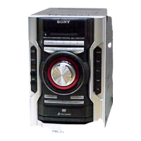
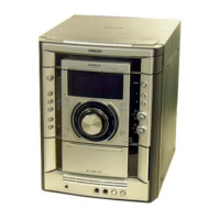
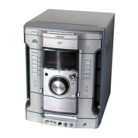
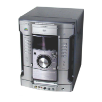
28
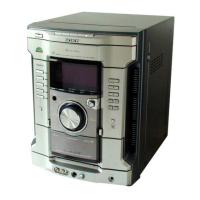
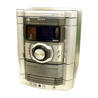
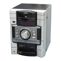
HCD-GNZ7D/GNZ8D/GNZ9D
SECTION 7
DIAGRAMS
• IC PIN Descriptions
IC101 M30392MEP-A00FPU (SYSTEM CONTROL) (PANEL BOARD (2/2))
Pin No. Pin Name I/O Pin Description
1 61537 CLK O TA device control serial clock signal output
2 61530 CLK O TA device control serial clock signal output
3TA DATA O TA device control serial data signal output
4STANDBY LED O Standby LED control signal output
5 VIDEO OUT SW O Video out switch control signal output “H”: VIDEO
6 VIDEO MUTE O Video mute signal output “L”: VIDEO
7 SIRCS I Remote control signal input
8VACS2 I VACS signal input
9 CN VSS — Connector ground pin
10 X CIN I Sub clock signal input (32.768 kHz)
11 X COUT O Sub clock signal output (32.768 kHz)
12 RESET I Reset signal input
13 XOUT O Main clock signal output (16 MHz)
14 VSS — Ground pin
15 X IN I Main clock signal input (16 MHz)
16 VCC1 — Power supply pin (+3.3 V)
17 P85 I Pull up (EVER+3.3 V)
18 ILLUMI 1/4 O Illumination on/off control signal output “H”: On
19 ST TUNED I ST tuned signal input
20 AC CUT I AC cut signal input
21 ILLUMI CTRL O Illumination control signal output
22 DVD POWER O DVD power supply control signal output
23 MTK RESET O MTK reset signal output
24 MTK BUSY O MTK busy signal output
25 I2C CLK I/O I2C serial clock signal input/output
26 I2C DATA I/O I2C serial data signal input/output
27 MTK OUT O MTK serial data signal output
28 MTK IN I MTK serial data signal input
29 MTK CLK I MTK serial clock signal input
30 MTK CS I MTK chip select signal input
31 to 43 G13 to G1 O Grid and segment control signal output
44 to 51 P1 to P8 O Grid and segment control signal output
52 VEE — Power supply pin
53 to 61 P9 to P17 O Grid and segment control signal output
62 VCC2 — Power supply pin (+3.3 V)
63 P18 O Grid and segment control signal output
64 VSS — Ground pin
65 to 67 P19 to P21 O Grid and segment control signal output
68 ST CE O Tuner chip enable signal output
69 ST DIN I Tuner data in signal input
70 ST DOUT O Tuner data out signal output
71 ST CLK O Tuner serial clock signal output
72 I/O VCC CONT O In/out power supply control signal output
73 I/O LATCH O In/out serial latch control signal output
74 WAKE UP0 I Wake up signal input
75 I/O CLK O In/out serial clock control signal output
76 I/O DI1 O In/out serial data control signal output
77 I/O RST O In/out reset signal output
78 TRG (B) O Tape mechanism logic (Trigger B) control signal output
79 TRG (A) O Tape mechanism logic (Trigger A) control signal output
80 ILLUMI 3/6 O Illumination on/off control signal output “H”: On
81 ILLUMI 2/3 O Illumination on/off control signal output “H”: On
82
PLAY SW (A) & (B)/
I
Head up switch detect signal input (A deck and B deck)
A-HALF A deck HALF signal input
w
w
w
.
x
i
a
o
y
u
1
6
3
.
c
o
m
Q
Q
3
7
6
3
1
5
1
5
0
9
9
2
8
9
4
2
9
8
T
E
L
1
3
9
4
2
2
9
6
5
1
3
9
9
2
8
9
4
2
9
8
0
5
1
5
1
3
6
7
3
Q
Q
TEL 13942296513 QQ 376315150 892498299
TEL 13942296513 QQ 376315150 892498299
http://www.xiaoyu163.com
http://www.xiaoyu163.com