EasyManua.ls Logo

Sony HCD-RG575 User Manual

Sony HCD-RG575
92 pages
To Next Page IconTo Next Page
Page #1 background imageLoading...
Page #1 background image
SERVICE MANUAL
COMPACT DISC DECK RECEIVER
US Model
Canadian Model
HCD-GX355/GX555
AEP Model
UK Model
Australian Model
HCD-RG270/RG475
E Model
HCD-RG270/RG475/RG575
HCD-GX355/GX555/
RG270/RG475/RG575
Ver. 1.2 2005.05
SPECIFICATIONS
9-879-533-03
2005E05-1
© 2005.05
Sony Corporation
Personal Audio Group
Published by Sony Engineering Corporation
Photo: HCD-RG575
HCD-GX355 is the amplifier, CD player, tape deck
and tuner section in MHC-GX355.
HCD-GX555 is the amplifier, CD player, tape deck
and tuner section in MHC-GX555.
HCD-RG270 is the amplifier, CD player, tape deck
and tuner section in MHC-RG270.
HCD-RG475 is the amplifier, CD player, tape deck
and tuner section in MHC-RG475S.
HCD-RG575 is the amplifier, CD player, tape deck
and tuner section in MHC-RG575S.
Amplifier section
AUDIO POWER SPECIFICATIONS
(HCD-GX555/GX355 USA model only)
HCD-GX555
POWER OUTPUT AND TOTAL HARMONIC
DISTORTION:
With 6 ohm loads, both channels driven, from
120 – 10,000 Hz: rated 145 watts per channel
minimum RMS power, with no more than 10%
total harmonic distortion from 250 milliwatts to
rated output.
HCD-GX355
POWER OUTPUT AND TOTAL HARMONIC
DISTORTION:
With 6 ohm loads, both channels driven, from
120 – 10,000 Hz: rated 150 watts per channel
minimum RMS power, with no more than 10%
total harmonic distortion from 250 milliwatts to
rated output.
North American model:
HCD-GX555
Front speaker
Continuous RMS power output (reference):
145 + 145 watts (6 ohms at
1 kHz, 10% THD)
Total harmonic distortion less than 0.07% (6 ohms at
1kHz, 80 W)
Sub woofer
Continuous RMS power output (reference):
170 watts (6 ohms at
80 Hz, 10% THD)
Total harmonic distortion less than 0.07% (6 ohms at
80 Hz, 90 W)
HCD-GX355
Continuous RMS power output (reference):
150 + 150 watts (6 ohms at
1 kHz, 10% THD)
Total harmonic distortion less than 0.07% (6 ohms at
1kHz, 80 W)
European and Russian models:
HCD-RG475
Front speaker
DIN power output (rated): 110 + 110 watts (6 ohms at
1kHz, DIN)
Continuous RMS power output (reference):
140 + 140 watts (6 ohms at
1kHz, 10% THD)
Music power output (reference):
280 + 280 watts (6 ohms at
1kHz, 10% THD)
Sub woofer
DIN power output (rated): 130 watts (6 ohms at
80 Hz, DIN)
Continuous RMS power output (reference):
160 watts (6 ohms at
80 Hz, 10% THD)
Music power output (reference):
320 watts (6 ohms at
80 Hz, 10% THD)
HCD-RG270
DIN power output (rated): 80 + 80 watts (6 ohms at
1kHz, DIN)
Continuous RMS power output (reference):
100 + 100 watts (6 ohms at
1kHz, 10% THD)
Music power output (reference):
200 + 200 watts (6 ohms at
1kHz,
10% THD)
– Continued on next page –
Model Name Using Similar Mechanism NEW
CD CD Mechanism Type
CDM74KFS-F1BD81C (Except Mexican model)/
CDM74KFS-F1BD84 (Mexican model)
Section
Base Unit Name BU-F1BD81C (Except Mexican model)/BU-F1BD84 (Mexican model)
Optical Pick-up Block Name KSM-215DCP
TAPE Model Name Using Similar Mechanism NEW
Section Tape Transport Mechanism Type CWM43FF13

Table of Contents

Question and Answer IconNeed help?

Do you have a question about the Sony HCD-RG575 and is the answer not in the manual?

Sony HCD-RG575 Specifications

General IconGeneral
BrandSony
ModelHCD-RG575
CategoryCar Receiver
LanguageEnglish

Summary

SPECIFICATIONS

North American model: AUDIO POWER SPECIFICATIONS

Power output specifications for North American models.

European and Russian models: HCD-RG475

Power output specs for European/Russian models.

CD player section

System Compact disc and digital audio system

Description of the CD player system.

Laser Diode Properties

Details about the laser diode.

Tape deck section

Recording system

Information on the tape recording system.

Tuner section

FM tuner section

Details on the FM tuner.

General

Power requirements

Electrical power specifications.

Power consumption

Electrical power usage details.

Inputs

AUDIO IN (stereo mini jack)

Description of audio input jack.

Outputs

PHONES (stereo mini jack)

Information about the headphone output.

SAFETY CHECK-OUT

LEAKAGE TEST

Procedure for testing AC leakage.

Notes on chip component replacement

Guidelines for replacing chip components.

Flexible Circuit Board Repairing

Specific repair instructions for flexible boards.

SAFETY-RELATED COMPONENT WARNING!!

Identifies critical safety components.

SERVICING NOTES

NOTES ON HANDLING THE OPTICAL PICK-UP BLOCK OR BASE UNIT

Handling precautions for the optical pick-up.

NOTES ON LASER DIODE EMISSION CHECK

Guidelines for checking laser diode emission.

MODEL IDENTIFICATION

Back Panel

Location of the model number label on the back panel.

GENERAL

Location of Controls

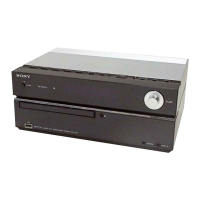
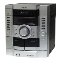
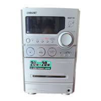
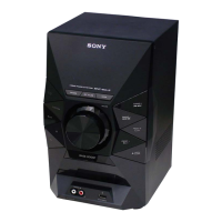
Identification of main unit controls.

DISASSEMBLY

DISASSEMBLY FLOW

Step-by-step process for disassembly.

TEST MODE

MC COLD RESET

Procedure to reset all data to initial conditions.

AM TUNING INTERVAL CHANGE-OVER

How to change AM tuning step between 9kHz and 10kHz.

CD SHIP (LOCK) MODE

Mode to secure pick-up position against vibration.

AMP TEST MODE

Procedure to display amplifier parameters and VACS status.

AGING MODE

CD section

Aging mode sequence for the CD section.

Tape Deck Section

Aging mode sequence for the tape deck section.

PANEL TEST MODE

Procedure

Steps to check fluorescent tube, LEDs, and buttons.

CD ERROR CODE DISPLAY MODE

Mechanism Deck Error Code Mode

Explains mechanism deck error codes.

Optical Pick-up Error Code Mode

Explains optical pick-up error codes.

REPEAT LIMIT CANCEL MODE

Mode to cancel CD repeat limit.

ELECTRICAL ADJUSTMENTS

S-CURVE CHECK

Procedure to check the S-curve waveform.

RFAC LEVEL CHECK

Procedure to check the RFAC signal level.

DIAGRAMS

BLOCK DIAGRAM - CD SERVO Section -

Block diagram of the CD servo circuitry.

BLOCK DIAGRAM - AUDIO/VIDEO Section -

BLOCK DIAGRAM - AMP Section -

BLOCK DIAGRAM - PANEL, POWER SUPPLY Section -

Note For Printed Wiring Boards and Schematic Diagrams

Note on Printed Wiring Board

Explains symbols and conventions for PWB diagrams.

Note on Schematic Diagram

Explains symbols and conventions for schematic diagrams.

Circuit Boards Location

PRINTED WIRING BOARD - CD Board - (Except MX model)

SCHEMATIC DIAGRAM - CD Board - (Except MX model)

PRINTED WIRING BOARD - BD Board - (MX model only)

SCHEMATIC DIAGRAM - BD Board - (MX model only)

PRINTED WIRING BOARDS - CHANGER Section

SCHEMATIC DIAGRAM - CHANGER Section -

PRINTED WIRING BOARD - MAIN Board -

SCHEMATIC DIAGRAM - MAIN Board (1/3) -

SCHEMATIC DIAGRAM - MAIN Board (2/3) –

SCHEMATIC DIAGRAM - MAIN Board (3/3) -

PRINTED WIRING BOARD - POWER Board -

SCHEMATIC DIAGRAM - POWER Board -

PRINTED WIRING BOARD - SUB WOOFER Board - (GX555/RG475/RG575 only)

SCHEMATIC DIAGRAM - SUB WOOFER Board - (GX555/RG475/RG575 only)

PRINTED WIRING BOARDS - AUDIO IN, MIC, HEADPHONE Boards -

SCHEMATIC DIAGRAM - AUDIO IN, MIC, HEADPHONE Boards

PRINTED WIRING BOARDS - CD-G Section - (MX model only)

SCHEMATIC DIAGRAM - CD-G Section - (MX model only)

PRINTED WIRING BOARD - PANEL Section (1/2) -

PRINTED WIRING BOARD - PANEL Section (1/2)

VOL BOARD

Printed wiring diagram for the Volume board.

SCHEMATIC DIAGRAM - PANEL Section (1/2) -

SCHEMATIC DIAGRAM - PANEL Section (2/2) -

PRINTED WIRING BOARDS - TRANS Section -

SCHEMATIC DIAGRAM - TRANS Section -

Waveforms

CD Board - (Except MX model)

Waveform details for the CD board (non-MX).

BD Board - (MX model only)

Waveform details for the BD board (MX model).

MAIN Board -

Waveform details for the main board.

IC Block Diagrams

CD Board - IC101 CXD3059AR

Block diagram for IC101 on the CD board.

DRIVER Board

IC701, 712 BA6956AN

Block diagram for IC701, 712 on the Driver board.

CD-G Board

IC1002 MSM514400E-60TS-K

Block diagram for IC1002 on the CD-G board.

IC1005 SN74AHCT04NSR

Block diagram for IC1005 on the CD-G board.

IC1006 NJM2561F1-TE2

Block diagram for IC1006 on the CD-G board.

MAIN Board

IC301 TC94A34FG-002

Block diagram for IC301 on the Main board.

CD-G Board

IC1001 TC9411AFG (BS, K) (CD GRAPHICS DECODER)

Block diagram for IC1001 on the CD-G board.

BD Board

IC101 CXD3059AR

Block diagram for IC101 on the BD board.

MAIN Board

IC101 BD3401KS2

Block diagram for IC101 on the Main board.

MIC Board

IC802 M65850FP-E1

Block diagram for IC802 on the MIC board.

IC Pin Function Description

MAIN BOARD M30302MCP-A02FPU0 (SYSTEM CONTROLLER)

Pinout description for the system controller IC.

CD-G BOARD IC1001 TC9411AFG (BS, K) (CD GRAPHICS DECODER)

PANEL BOARD IC701 μPD780232GC-508-8BT-A (FL/LED DRIVER)

EXPLODED VIEWS

OVERALL SECTION

Exploded view of the entire unit with part numbers.

BACK PANEL SECTION

FRONT PANEL SECTION

KEY SECTION

CHASSIS SECTION

TRANSFORMER SECTION

CD MECHANISM DECK SECTION-1

CD MECHANISM DECK SECTION-2

ELECTRICAL PARTS LIST

RESISTORS

List of resistors with part numbers and values.

SEMICONDUCTORS

List of semiconductors with part numbers.

CAPACITORS

List of capacitors with part numbers and values.

COILS

List of coils with part numbers.

REVISION HISTORY

Related product manuals