Home
Sony
Receiver
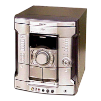
HCD-RV333D
Sony HCD-RV333D User Manual
4
of 1
of 1 rating
102 pages
Give review
Manual
Specs
To Next Page
To Next Page
To Previous Page
To Previous Page
Loading...
HCD-RV222D/R
V222DL/RV333D/RV333DL/R
V555D
HCD-RV222D/R
V222DL/RV333D/R
V333DL/RV555D
39
39
5-1
1.
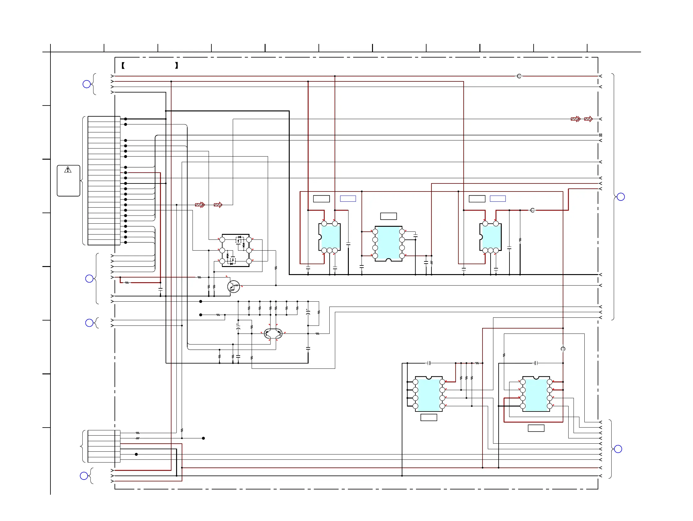
SCHEMA
TIC DIAGRAM – DMB19 Section (1/4) –
(3/4)
DMB19
3
BOARD
DMB19
BOARD
(3/4)
4
DMB19
BOARD
(3/4)
5
DMB19
BOARD
(4/4)
6
BOARD
(2/4)
1
DMB19
DMB19
(2/4)
BOARD
2
IC B/D
IC B/D
0
0
0
0
0
1.3
1.3
0
1.6
1.6
3.2
3.2
00
5
3.3
3.2
1.3
3.2
3.2
0.5
1.8
5
3.3
3.2
1.3
3.2
3.3
3.2
3.2
0.4
0
3.2
3.2
3.2
0
0
6P
CN105
TXD
RXD
GND
+3.3V
V2REFO
RFMON
47k
R124
0.01
C192
54
3
2
1
+3.3V REG
CONT
GND
NOISE
VOUT
VIN
0.5%
22
R1
12
2.7k
R
1110
100k
R1
14
100
R109
0.01
C1
13
0.5%
22
R1
15
100
R101
10k
R107
10V
47
C105
1k
R193
0.22
C195
47k
R1
17
C182
0.22
1k
R1
16
0.01
C101
22
R121
C184
0.01
10V
47
C1
12
1M
R108
1
2
3
4
5
6
7
8
9
10
11
12
13
14
15
16
17
18
19
20
21
22
23
24
CN101
24P
GND (LD)
LD (650)
NC
NC
PD
LD (780)
VR (650)
VR (780)
NC
VOE/E+G
VCC
VC
GND (PDIC)
VOF/F+H
VOB/B
VOA/A
RF
(LO:DVD.HI:CD)MSW
VOD/D
VOC/C
TRK-
TRK+
FCS+
FCS-
0.01
C106
0.5%
22
R1
13
54
3
2
1
TK1
1133CSCL-G
IC107
CONT
GND
NOISE
VOUT
VIN
100
R123
1k
R191
47k
R1
10
0.22
C193
22
R1
18
22
R120
100k
R1
129
100
R
111
Q102
QST8TR
LASER DRIVER CONTROL
JL1
101
JL1
102
JL1
105
JL1
106
JL1
107
JL1
108
J
L111
0
J
L1111
J
L111
2
J
L111
3
J
L111
4
J
L111
5
J
L111
6
J
L111
7
J
L111
8
J
L111
9
JL1
120
JL1
121
JL1
122
JL1
123
JL1
124
CL106
CL107
REG01
TRK-
TRK+
FCS+
FCS-
REG02
IOP
IOPMON
VREFO
RF+3.3V
DVDD5V
DGND
C188
470p
1
C198
1
C183
1k
R1178
DGND
C186
0.22
R151
10k
FB1
12
0.01
C1
130
10k
R135
R102
0
S-24CS16A0I-J8T1G
IC103
EEPROM
A0
A1
A2
GND
SDA
SCL
WE
VCC
MX25L1605DM2I-12G
IC102
SF-ROM
_CS
SO
_W
GND
SI
SCK
_HOLD
VCC
DVDD3.3V
CL105
V2REFO
0
R1
192
1000p
C102
FB1
10
0
R1253
8
7
6
54
3
2
1
MM1661JHBE
I
C111
VO
NC
GND
CN
FB109
CL1
152
R1280
0
DGND
DVDD5V
1
2
3
4
BUS1
5
6
7
8
9
10
11
12
13
14
15
16
17
18
19
21
22
23
24
CD_LD
DVD_LD
(1/2)
PICK-UP
OPTICAL
BLOCK
LINE-JIG
)
(
FOR
IC105
IC103
IC102
81
0
F
B
6
3
D
7
E
9
G
C
2
1
H
11
5
4
A
1
2
3
4
5
6
8
7
6
5
4
3
2
1
8
7
6
5
4
3
2
1
D1
G2
S2
D2
G1
S1
(1/4)
DMB19 BOARD
DVD_LD
CD_LD
VOE
VOF
VOB
VOA
VOD
TRK-
TRK+
FCS+
FCS-
TRK-
TRK+
FCS+
FCS-
RT1N241C-TP-1
Q103
MEDIA SWITCH CONTROL
UM6K1N-TN
Q101
MEDIA SWITCH CONTROL
CONT
NC
NC
VIN
+3.3V REG
IC107
+1.8V REG
I
C
111
TK1
1133CSCL-G
IC105
• See page 65 for IC Block Diagrams.
(Page 41)
(Page 41)
(Page 41)
(Page 42)
(Page 40)
(Page 40)
38
40
Table of Contents
Default Chapter
5
Table of Contents
5
1 Servicing Notes
6
2 Disassembly
8
Case
9
VOL-LED Board
9
Tuner Assy
10
Loading Panel
10
DVD Block
11
Front Panel Section
11
Back Panel Section
12
MAIN Board
12
2CH-AMP Board (RV222D/RV222DL/RV555D), 3CH-AMP Board (RV333D/RV333DL)
13
Tape Mechanism Block
13
JACK-MIC AMP Board
14
Lid (TC-L), Lid (TC-R)
14
TC AMP Board
15
PANEL Board
15
KEY-RIGHT Board
16
KEY-LEFT Board
16
DMB19 Board
17
Base Unit
17
Optical Pick-Up
18
DRIVER Board, SW Board
18
SENSOR Board
19
MOTOR (TB) Board
19
MOTOR (LD) Board
20
3 Test Mode
21
4 Electrical Adjustments
26
5 Diagrams
27
Block Diagram -RF Section
28
Block Diagram -DVD out Section
29
Block Diagram -Audio Section
30
Block Diagram -Tape Section
31
Block Diagram -AMP Section
32
Block Diagram -Power Section
33
Printed Wiring Boards -Driver Section
35
Schematic Diagram -Driver Section
36
Printed Wiring Board -DMB19 Section (1/2)
37
Printed Wiring Board -DMB19 Section (2/2)
38
Schematic Diagram -DMB19 Section (1/4)
39
Schematic Diagram -DMB19 Section (2/4)
40
Schematic Diagram -DMB19 Section (3/4)
41
Schematic Diagram -DMB19 Section (4/4)
42
Printed Wiring Boards -Reg/Tuner Section
43
Schematic Diagram -REG Section
44
Schematic Diagram -Tuner Section
45
Printed Wiring Board -Main Section
46
Schematic Diagram -Main Section (1/3)
47
Schematic Diagram -Main Section (2/3)
48
Schematic Diagram -Main Section (3/3)
49
Printed Wiring Board -Jack-MIC AMP Section
50
Schematic Diagram -Jack-MIC AMP Section
51
Printed Wiring Board -TC AMP Section
52
Schematic Diagram -TC AMP Section
53
Printed Wiring Boards -Panel Section
54
Printed Wiring Boards -Key-Left/Key-Right Section
55
Schematic Diagram -Panel Section
56
Printed Wiring Board -2CH-AMP Section (RV222D/RV222DL/RV555D)
57
Schematic Diagram -2CH-AMP Section (RV222D/RV222DL/RV555D)
58
Printed Wiring Board -3CH-AMP Section (RV333D/RV333DL)
59
Schematic Diagram -3CH-AMP Section (RV333D/RV333DL)
60
Printed Wiring Board -Power Section (RV222D/RV222DL)
61
Schematic Diagram -Power Section (RV222D/RV222DL)
62
Printed Wiring Board -Power Section (RV333D/RV333DL/RV555D)
63
Schematic Diagram -Power Section (RV333D/RV333DL/RV555D)
64
6 Exploded Views
74
Overall Section
74
Front Panel Section-1
75
Front Panel Section-2
76
Chassis Section
77
DVD Section
78
DVD Mechanism Deck Section-1
79
DVD Mechanism Deck Section-2
80
7 Electrical Parts List
81
4
Based on 1 rating
Ask a question
Give review
Questions and Answers:
Need help?
Do you have a question about the Sony HCD-RV333D and is the answer not in the manual?
Ask a question
Sony HCD-RV333D Specifications
General
Tuner
FM/AM
Audio Formats Supported
MP3
Outputs
Headphone Jack
Remote Control
Yes
Disc Playback
CD
Inputs
Auxiliary
Type
Mini Hi-Fi System
Related product manuals
Sony HCD-RV990D
120 pages
Sony HCD-RV777D
120 pages
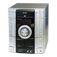
Sony HCD-RV222D
102 pages
Sony HCD-RV660D
120 pages
Sony HCD-RV888D
120 pages
Sony HCD-RV999D
120 pages
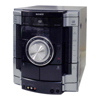
Sony HCD-RV555D
102 pages
Sony HCD-SLK1i - Dvd Receiver
88 pages
Sony HCD-FR1
138 pages
Sony HCD-xb5
94 pages
Sony HCD-SC6
126 pages
Sony HCD-FL5D
156 pages
 Loading...