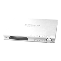
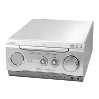
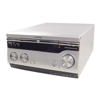
HCD-S888
3232
Note on Schematic Diagram:
• All capacitors are in µF unless otherwise noted. pF: µµF
50 WV or less are not indicated except for electrolytics
and tantalums.
• All resistors are in Ω and
1
/
4
W or less unless otherwise
specified.
• f : indicates tolerance.
• 2 : nonflammable resistor.
• C : panel designation.
• A : B+ Line.
•Voltages and waveforms are dc with respect to
groundunder no-signal (detuned) conditions.
no mark : DVD PLAY
():CD PLAY
[]:SACD PLAY
•Voltages are taken with a VOM (Input impedance 10 MΩ).
Voltage variations may be noted due to normal produc-
tion tolerances.
•Waveforms are taken with a oscilloscope.
Voltage variations may be noted due to normal produc-
tion tolerances.
• Circled numbers refer to waveforms.
• Signal path.
J : CD PLAY
c : DVD PLAY
I : SACD PLAY
f : AUX IN
i : OPTICAL DEITAL IN
d : TUNER
F : AUDIO
L : VIDEO
E : Y
a : CHROMA
r : COMPONENT VIDEO
6-2. Note For Printed Wiring Boards And Schematic Diagrams
Note on Printed Wiring Board:
• X : parts extracted from the component side.
• Y : parts extracted from the conductor side.
• f : indicates tolerance.
• : Pattern from the side which enables seeing.
(The other layers' patterns are not indicated.)
Caution:
Pattern face side: Parts on the pattern face side seen from
(Side B) the pattern face are indicated.
Parts face side: Parts on the parts face side seen from
(Side A) the parts face are indicated.
• Indication of transistor.
Note: The components identified by mark 0 or dotted line
with mark 0 are critical for safety.
Replace only with part number specified.
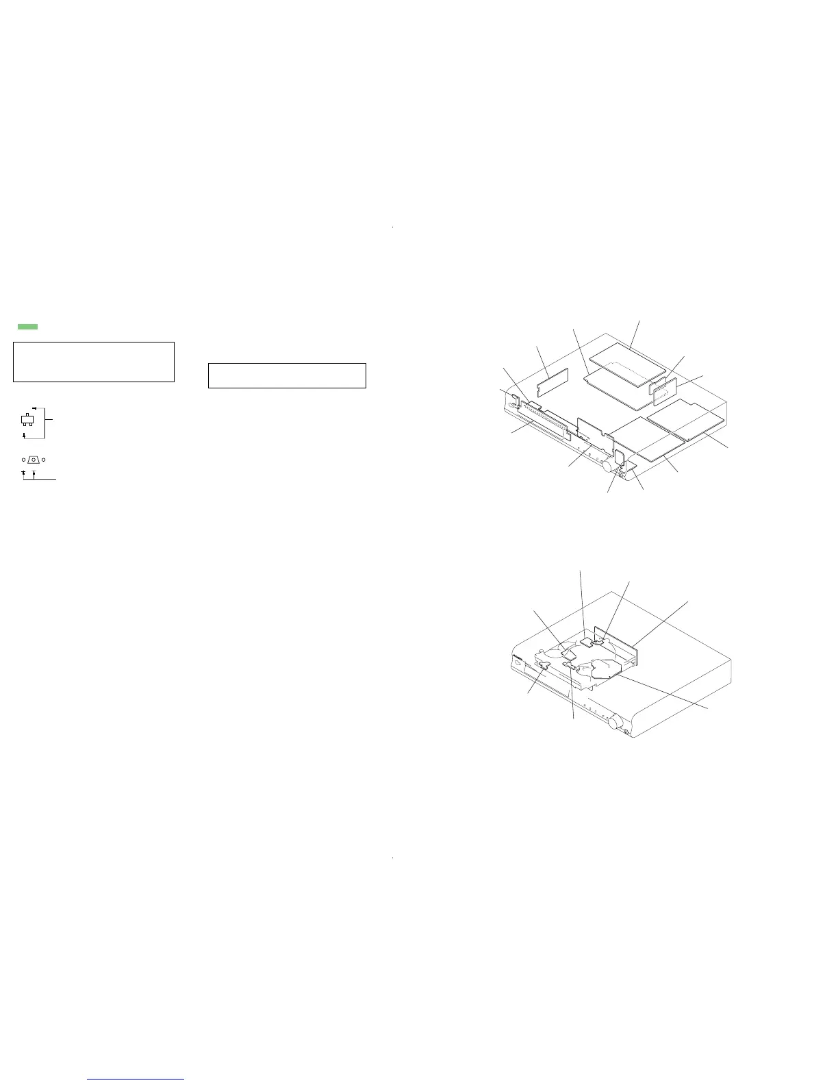
FL board
DDCON board
CONTROL board
VOL board
HP board
DVD board
POWER board
AMP boar