– 22 –
SECTION 7
DIAGRAMS
7-1. IC PIN FUNCTION DESCRIPTION
• MAIN BOARD IC301 µPD780018YGF-028-3BA (SYSTEM CONTROLLER)
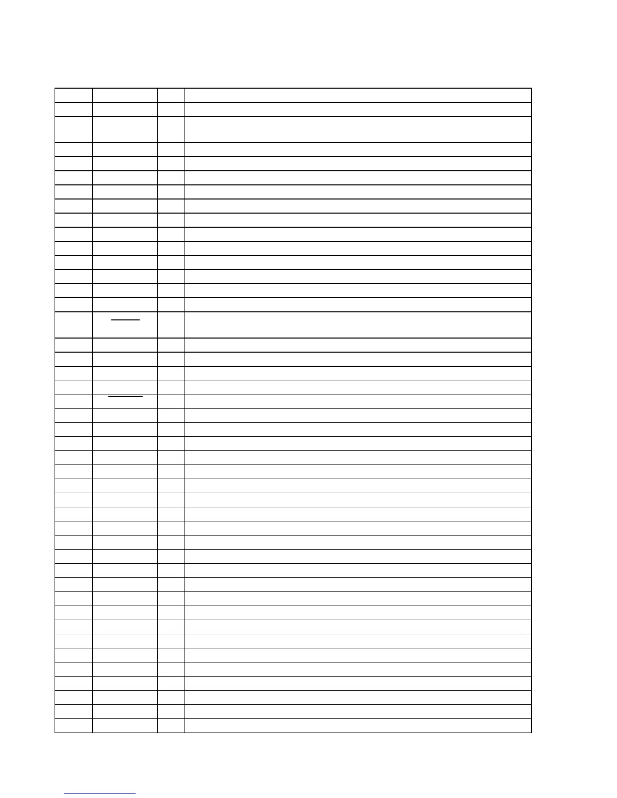
Pin No. Pin Name I/O Function
1 TA-MUTE O
Line muting on/off control signal output terminal “L”: muting on
2 DBFB-H/L O
DBFB normal/high selection signal output to the M62427FP (IC201)
“L”: DBFB high, “H”: DBFB low
3 427-LAT O
Serial data latch pulse output to the M62427FP (IC201)
4 K-CON-LAT O
Serial data latch pulse output terminal Not used (open)
5 K-CON-ON O
On/off selection signal output of the key control circuit “L”: on Not used (open)
6 F-RELAY O
Relay drive signal output for the speaker protect “H”: on
7 R-RELAY O
Relay drive signal output for the speaker protect “H”: on Not used (open)
8 PL-RELAY O
Relay drive signal output for the speaker protect “H”: on Not used (open)
9 TEST I
Test terminal Connected to ground
10 X2 O
Main system clock output terminal (5 MHz)
11 X1 I
Main system clock input terminal (5 MHz)
12 VDD —
Power supply terminal (+5V)
13 XT2 O
Sub system clock output terminal (32.768 kHz)
14 XT1 I
Sub system clock input terminal (32.768 kHz)
15 RESET I
System reset signal input from the reset signal generator (IC302) “L”: reset
For several hundreds msec. after the power supply rises, “L” is input, then it changes to “H”
16 (INT/IN) I
Connected to ground
17 (INT/IN/OUT) I
Connected to ground
18 SCOR I
Subcode sync (S0+S1) detection signal input from the CXD2519Q (IC103)
19 SOFT-TEST O
Output terminal for the software test (open)
20 AC-CUT I
AC off detection signal input from the reset signal generator (IC302)
21 RDS-INT I
Serial data reading clock signal input for the radio data system Not used (fixed at “L”)
22 RDS-DATA I
Serial data input for the radio data system Not used (open)
23 VDD —
Power supply terminal (+5V)
24 AVDD —
Power supply terminal (+5V) (for A/D conversion)
25 ADJ I
Setting terminal for the CD test mode Normally: fixed at “H”
26 A-SHUT I
Shut off detection signal input from the deck-A side reel pulse detector (Q1001)
27 B-SHUT I
Shut off detection signal input from the deck-B side reel pulse detector (Q1002)
28 B-HALF I
Detection input from the deck-B half detect switch (S1006)
29 CLK-CHECK I
Not used (fixed at “L”)
30 SPEC-IN I
Setting terminal for the version
31 ADJ2 I
Setting terminal for the CD test mode Normally: “L”
32 DEMO-MODE I
Setting terminal for the demonstration H/L Fixed at “L”
33 AVSS —
Ground terminal (for A/D conversion)
34 SQ-DATA-IN I
Sub-code Q data input from the CXD2519Q (IC103)
35 NCO O
Not used (open)
36
SQ-CLK
O
Sub-code Q data reading clock signal output to the CXD2519Q (IC103)
37
SW-ON/OFF
O
Super woofer speaker on/off control signal output terminal Not used (open)
38
FUNC1
I
Setting terminal for the function 1 Fixed at “L”
39 FUNC2 I
Setting terminal for the function 2 Fixed at “L”
40 VSS —
Ground terminal
41 VOL-LAT O
Serial data latch pulse output terminal Not used (open)
42 PL-LAT O
Serial data latch pulse output terminal Not used (open)
43 COM-DIN I
Serial data input terminal Not used (fixed at “L”)


 To Next Page