10
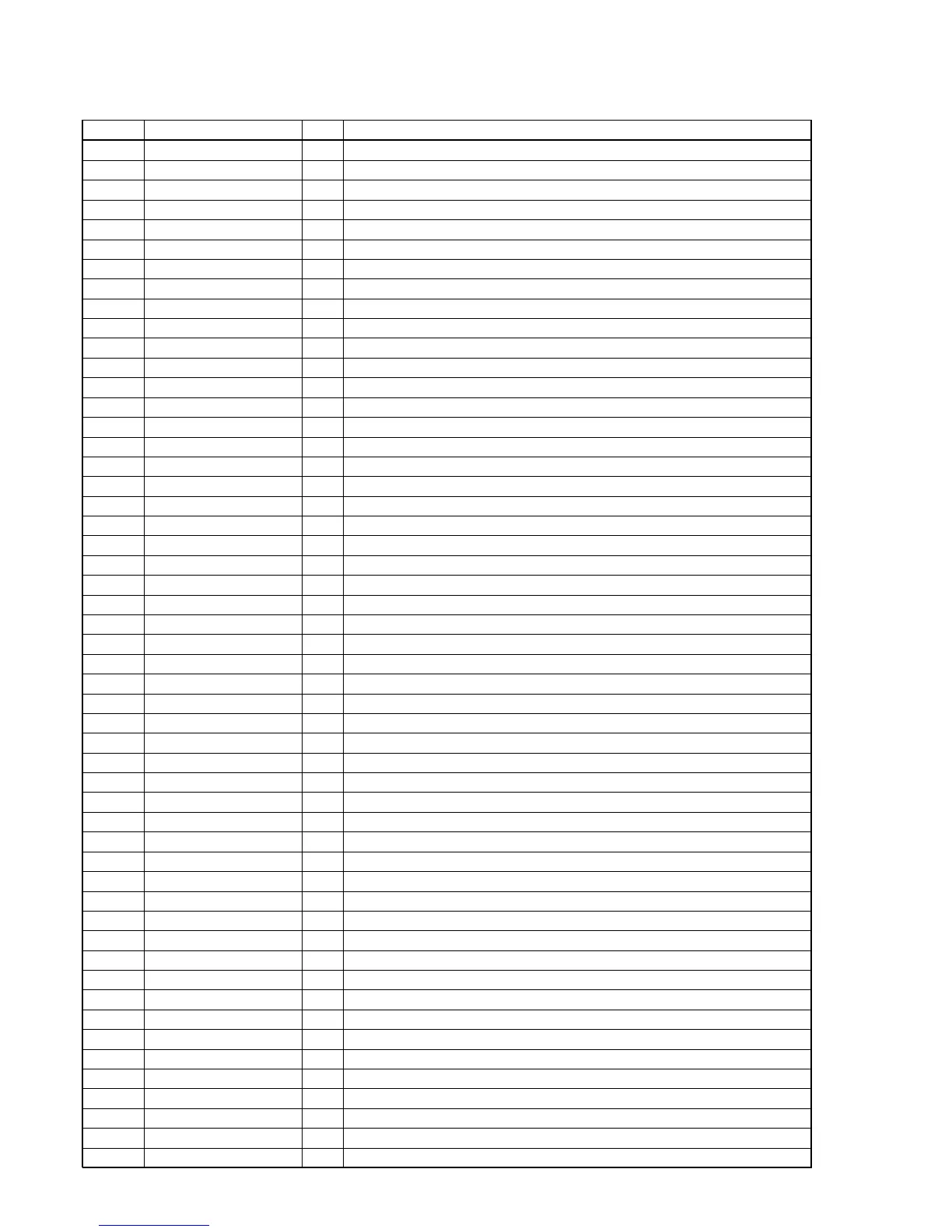
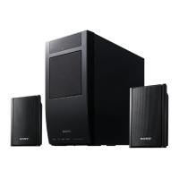
HT-BE1/SA-WBE1/SS-BE1
1 VSS — Ground
2 XRST I Reset signal input from system controller.
3 EXTIN I Not used. (Connected to ground)
4 FS2 I Not used. (Connected to ground)
5 VDDI I Power supply pin (+2.4 V)
6 FS1 I Not used. (Connected to ground)
7 PLOCK O Internal PLL lock signal output for system controller.
8 VSS — Ground
9 MCLK1 I Clock signal input (13.5 MHz)
10 VDDI I Power supply pin (+2.4 V)
11 VSS — Ground
12 MCLK2 O Clock signal output (13.5 MHz)
13 MS I Switching signal input of master/slave operation. (Fixed at L : internal clock)
14 SCKOUT O Internal system clock signal output
15 LRCKI1 I Not used. (open)
16 VDDE I Power supply pin (+3.3 V)
17 BCKI1 I Not used. (open)
18 SDI1 I Audio IF data input
19 LRCKO O Sampling clock output for digital audio serial data
20 BCKO O Bit clock output for digital audio serial data
21 VSS — Ground
22 KFSIO I/O Audio clock signal (384fs/256fs) input/output
23 to 25 SDO1 to SDO3 O Digital audio serial data output
26 SDO4 O Audio IF serial output (Not used. (open))
27 SPDIF O Not used. (open)
28 LRCKI2 I Sampling clock input from audio serial data.
29 BCKI2 I Bit clock input from audio serial data.
30 SDI2 I Digital audio data input
31 VSS — Ground
32 HACN O Acknowledge signal output for system controller.
33 HDIN I Serial data input from system controller.
34 HCLK I Clock input from system controller.
35 HDOUT O Serial data output for system controller.
36 HCS I Chip select input from system controller.
37 SDCLK O Not used. (open)
38 CLKEN O Not used. (open)
39 RAS O Not used. (open)
40 VDDI I Power supply pin (+2.4 V)
41 VSS — Ground
42 CAS O Not used. (open)
43 DQM/OE0 O Not used. (open)
44 CS0 O External memory chip select output (SRAM) (Not used. (open))
45 WE0 O SRAM write enable output (Not used. (open))
46 VDDE I Power supply pin (+3.3 V)
47 WMD1 I Not used. (Fixed at L)
48 VSS — Ground
49 WMD0 I Not used. (Fixed at L)
50 PAGE2 O Not used. (open)
51 VSS — Ground
52 PAGE1 O External memory page switching signal output (Not used. (open))
53 PAGE0 O External memory page switching signal output (Not used. (open))
54 BOOT I Not used. (open)
• IC802 CXD9617R (DSP)
Pin No. Pin Name I/O Pin Description