11 11
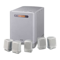
HT-BE1/SA-WBE1/SS-BE1
Note on Schematic Diagram:
• All capacitors are in µF unless otherwise noted. (p: pF)
50 WV or less are not indicated except for electrolytics
and tantalums.
• All resistors are in Ω and
1
/
4
W or less unless otherwise
specified.
• 2 : nonflammable resistor.
• C : panel designation.
Note:
The components identi-
fied by mark 0 or dotted
line with mark 0 are criti-
cal for safety.
Replace only with part
number specified.
Note:
Les composants identifiés par
une marque 0 sont critiques
pour la sécurité.
Ne les remplacer que par une
piéce portant le numéro
spécifié.
• A : B+ Line.
•Voltage is dc with respect to ground under no-signal
(detuned) condition.
•Voltages are taken with a VOM (Input impedance 10 MΩ).
Voltage variations may be noted due to normal produc-
tion tolerances.
• Signal path.
F : LINE
c : DIGITAL AUDIO (OPTICAL)
J : DIGITAL AUDIO (COAXIAL)
• Abbreviation
CND : Canadian model.
SP : Singapore model.
MY : Malaysia model.
MX : Mexican model.
•( ): Page of Service Manual.
(( )) : Page of Supplement-1.
Note on Printed Wiring Boards:
• X : parts extracted from the component side.
• : Pattern from the side which enables seeing.
• Abbreviation
CND : Canadian model.
SP : Singapore model.
MY : Malaysia model.
MX : Mexican model.
•( ): Page of Service Manual.
(( )) : Page of Supplement-1.
55 BTACT O Not used. (open)
56 BST I Boot stop signal input from system controller.
57 MOD1 I Operation mode signal input (Fixed at H : 256fs)
58 MOD0 I Operation mode signal input (Fixed at L : single chip mode)
59 EXLOCK I Lock signal input
60 VDDI I Power supply pin (+2.4 V)
61 VSS — Ground
62 to 66 A17 to A13 O External memory address output (SRAM) (Not used. (open))
67 GP10 O Connected to LRCKO
68 GP9 O Decode signal output for system controller.
69 GP8 I Audio signal input from DIR.
70 VDDI I Power supply pin (+2.4 V)
71 VSS — Ground
72 to 75 D15/GP7 to D12/GP4 I/O External memory data input/output (general port) (Not used. (open))
76 VDDE I Power supply pin (+3.3 V)
77 to 80 D11/GP3 to D8/GP0 I/O External memory data input/output (general port) (Not used. (open))
81 VSS — Ground
82 A9 O External memory address output (SRAM) (Not used. (open))
83 to 85 A12 to A10 O External memory address output (SRAM) (Not used. (open))
86 TDO O Not used. (open)
87 TMS I Not used. (open)
88 XTRST I Not used. (open)
89 TCK I Not used. (open)
90 TDI I Not used. (open)
91 VSS — Ground
92 to 97 A8 to A3 O External memory address output (SRAM) (Not used. (open))
98, 99 D7, D6 I/O External memory data input/output (SRAM) (Not used. (open))
100 VDDI I Power supply pin (+2.4 V)
101 VSS — Ground
102 to 105 D5 to D2 I/O External memory data input/output (SRAM) (Not used. (open))
106 VDDE I Power supply pin (+3.3 V)
107, 108 D1, D0 I/O External memory data input/output (SRAM) (Not used. (open))
109, 110 A2, A1 O External memory address output (SRAM) (Not used. (open))
111 VSS — Ground
112 A0 O External memory address output (SRAM) (Not used. (open))
113 PM I PLL initialization input from system controller.
114, 115 SDI3, SDI4 I Not used. (open)
116 SYNC I Sync/async selection input (Fixed at H : async)
117 to 119 VSS — Ground
120 VDDI I Power supply pin (+2.4 V)
Pin No. Pin Name I/O Pin Description
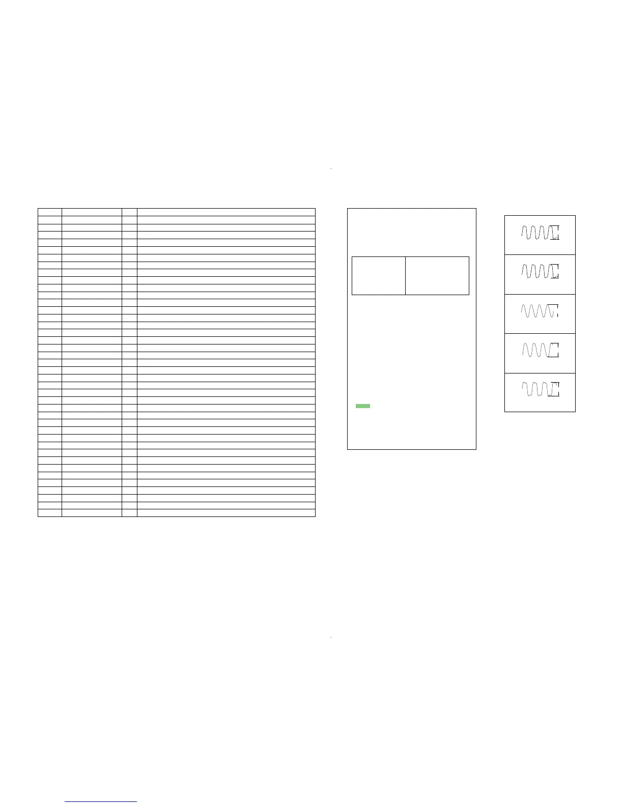
• Waveforms
1
IC501
wk
(XT0)
1V/div 50nsec/div
12.0MHz
2
IC803
wa
(XOUT)
1V/div 50nsec/div
12.288MHz
3
IC801
ek
(X2)
1V/div 20nsec/div
4
IC802
qs
(MCLK2)
1V/div 50nsec/div
16.0MHz
13.5MHz
5
IC802
qf
(SCKOUT)
1V/div 50nsec/div
13.5MHz
3.0Vp-p
3.5Vp-p
2.6Vp-p
3.1Vp-p
4.0Vp-p
Ver. 1.3