10
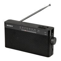
ICF-C630
SECTION 5
DIAGRAMS
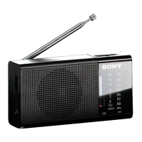
1
2 3
4
5 6 7 8 9
10
15141312
11
FM
DISCRIMINATOR
AF POWER AMP AM FE FM IF
TUNING
METER
AM IF DET AGC
FM FE
23 22 21 202425 19 18 17 1629 28 27 2630
GND
GND
AF OUT
+B
RIPPLE
FILTER
AF IN
DET OUT
AFC (J)AGC
AFC (W)AGC
IF GND
LED
NC
FM IF IN
AM IF IN
BAND SW
NC
MIX OUT
FE GND
AM ANT
FM RF
REG
FM OSC
FM ANT
AFC
AM OSC
VOL
NF
DISCRI
GND
GND
IC1 CXA1019S
5-1. IC BLOCK DIAGRAM
THIS NOTE IS COMMON FOR PRINTED WIRING
BOARDS AND SCHEMATIC DIAGRAMS.
Common Note on Schematic Diagram:
• All capacitors are in µF unless otherwise noted. pF: µµF
50 WV or less are not indicated except for electrolytics
and tantalums.
• All resistors are in Ω and
1
/
4
W or less unless otherwise
specified.
•
f
: internal component.
• C : panel designation.
• A : B+ Line.
• H : adjustment for repair.
• Power voltage is dc 4.5V and fed with regulated dc power
supply from external power voltage jack.
•Voltage is dc with respect to ground under no-signal
(detuned) condition.
no mark : FM
(): AM
•Voltages are taken with a VOM (Input impedance 10 MΩ).
Voltage variations may be noted due to normal produc-
tion tolerances.
• Signal path.
F : FM
f : AM
Note: The components identified by mark 0 or dotted line
with mark 0 are critical for safety.
Replace only with part number specified.
Common Note on Printed Wiring Boards:
• X : parts extracted from the component side.
• Y : parts extracted from the conductor side.
•
f
: internal component.
• : Pattern from the side which enables seeing.