2
SAFETY-RELATED COMPONENT WARNING!!
COMPONENTS IDENTIFIED BY MARK 0 OR DOTTED LINE
WITH MARK 0 ON THE SCHEMATIC DIAGRAMS AND IN
THE PARTS LIST ARE CRITICAL TO SAFE OPERATION.
REPLACE THESE COMPONENTS WITH SONY PARTS WHOSE
PART NUMBERS APPEAR AS SHOWN IN THIS MANUAL OR
IN SUPPLEMENTS PUBLISHED BY SONY.
Notes on Chip Component Replacement
• Never reuse a disconnected chip component.
• Notice that the minus side of a tantalum capacitor may be dam-
aged by heat.
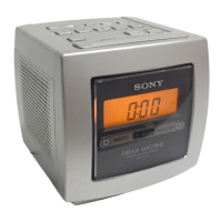
ICF-C630
TABLE OF CONTENTS
1. SERVICING NOTES
1-1. Dial Pointer Setting ............................................................. 3
1-2. Installing the Tuner Board ................................................... 3
2. GENERAL
Choosing Power Sources ......................................................... 4
Setting the brightness of the backlight .................................... 4
Setting the Clock ..................................................................... 4
Improving the reception .......................................................... 4
Operating the Radio................................................................. 4
Setting the Alarm ..................................................................... 4
Setting the Sleep Timer ........................................................... 4
Using the NAP Timer (Count Down Timer) ........................... 4
3. DISASSEMBLY
3-1. Cover Assy .......................................................................... 5
3-2. Tuner Board......................................................................... 6
3-3. Cabinet (Upper) Assy .......................................................... 6
3-4. Microcomputer Board, Key (Left) Board,
Key (Right) Board ............................................................... 7
4. ELECTRICAL ADJUSTMENTS................................... 8
5. DIAGRAMS
5-1. IC Block Diagram ............................................................. 10
5-2. Block Diagram .................................................................. 11
5-3. Printed Wiring Board –Tuner Section– ............................. 12
5-4. Printed Wiring Boards –Micon Section– .......................... 13
5-5. Schematic Diagram ........................................................... 14
5-6. IC Pin Description............................................................. 15
6. EXPLODED VIEWS
6-1. Cabinet (Lower) Section ................................................... 16
6-2. Cover Assy Section ........................................................... 17
7. ELECTRICAL PARTS LIST ........................................ 18