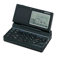
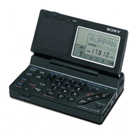
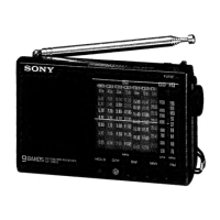
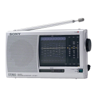
ICF-SW11
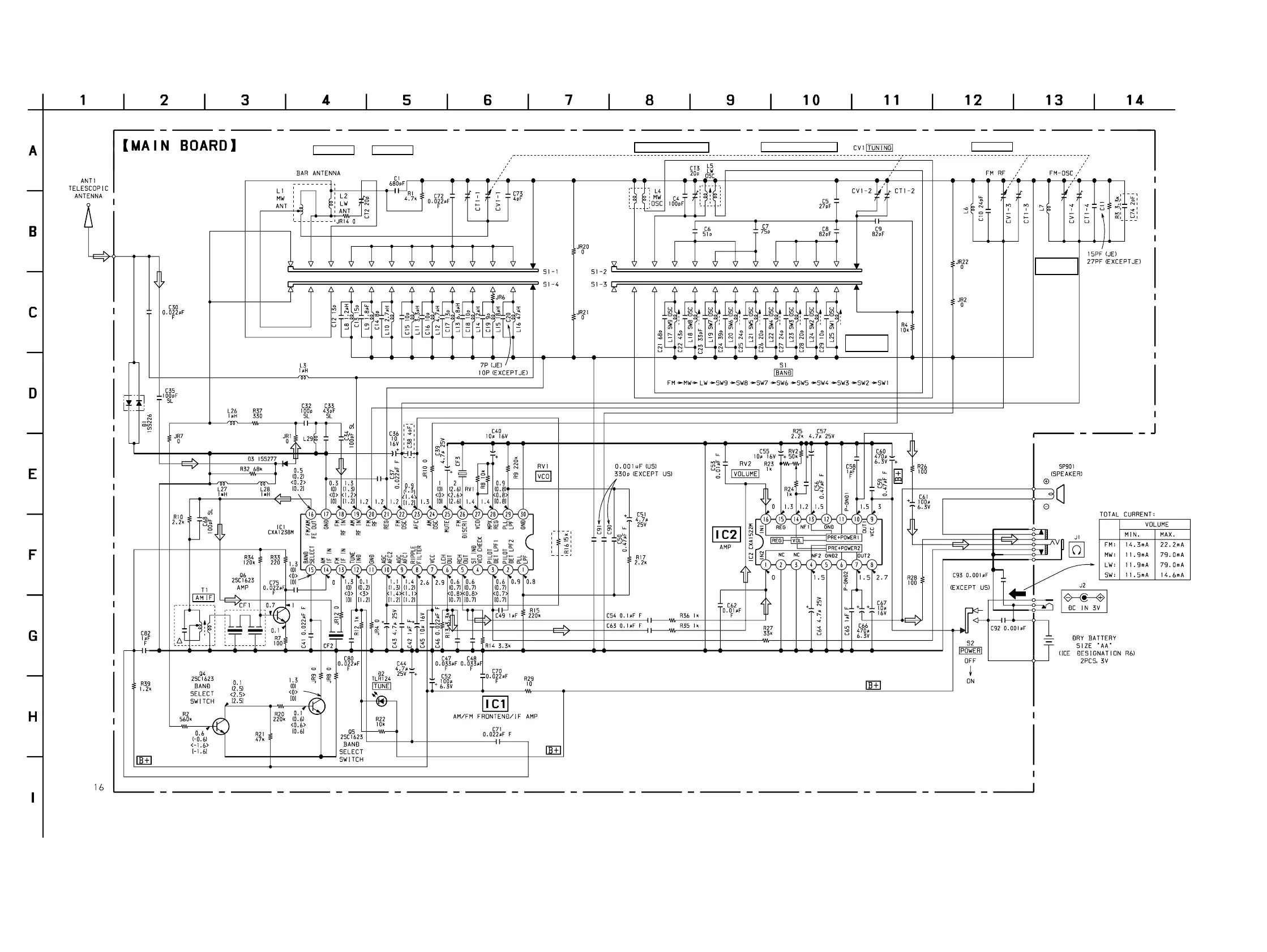
4-3. SCHEMATIC DIAGRAM
— 11 — — 12 —
L7,CT1-4
FM FREQUENCY
COVERAGE
L17-L25
SW FREQUENCY
COVERAGE
L6, CT1-3
FM TRACKING
L4, CT1-2L5, CT3
MW FREQUENCY COVERAGE
LW FREQUENCY COVERAGE
L1, CT1-1
MW TRACKING
L2, CT2
LW TRACKING
EXCEPT
JE
MODEL
EXCEPT JE
MODEL
(JE)
27µH(EXCEPT JE)
JE MODEL
Note on Schematic Diagram:
• All capacitors are in µF unless otherwise noted. pF: µµF
50 WV or less are not indicated except for electrolytics
and tantalums.
• All resistors are in Ω and
1
/
4
W or less unless otherwise
specified.
•
f
: internal component.
• U : B+ Line.
• C : panel designation.
• H : adjustment for repair.
no mark :
( ) : MW
< > : SW
[]: LW
• Voltages are taken with a VOM (Input impedance 10 MΩ).
Voltage variations may be noted due to normal production
tolerances.
• Signal path.
F : FM
• Abbreviation
JE : Tourist model
• Refer to page 8 for IC Block Diagrams.