Do you have a question about the Sony MDS-JB920 and is the answer not in the manual?
Details input signal types, impedance, and rated input for the audio system.
Details output signal types, load impedance, and rated output for the audio system.
Describes the deck's diagnostic display showing condition and messages.
Steps to enter and use the self-diagnosis error history display mode.
Details of displays like total rec, total play, retry err, total err, err history.
Lists error codes and their corresponding error details for diagnosis.
Essential safety checks before releasing the unit to the customer.
Method for measuring and ensuring AC leakage does not exceed limits.
Information on identifying different model versions and part numbers.
Cautions regarding laser exposure and battery replacement hazards.
Guidelines for safe repair, including flexible circuit board and chip component handling.
Description and use of a special jig for checking BD board waveforms.
Procedure to record IOP values onto non-volatile memory.
Procedure to read IOP values from non-volatile memory.
Procedures for determining faulty locations before replacing parts.
Steps to reset the system microprocessor when the unit is unresponsive.
Procedure for entering and using the test mode to diagnose retry causes.
Explanation of how to interpret the displayed retry cause information.
Table for converting hexadecimal values to binary for display interpretation.
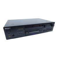
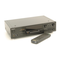
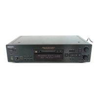
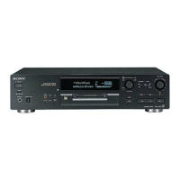
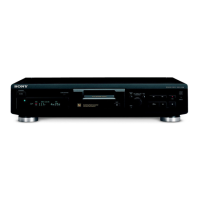
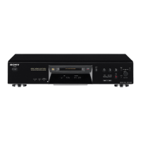
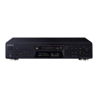
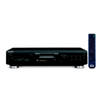
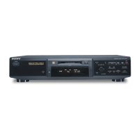
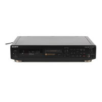
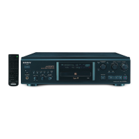
Identifies and describes the location of all front and rear panel controls.
Instructions for connecting the MD deck to other audio components.
Explanation of the CONTROL A1 system's functionality and compatibility.
Details automatic function selection and synchronized recording features.
Procedure for setting the internal clock for accurate date/time stamping.
Step-by-step guide for disassembling the main chassis of the unit.
Procedures for removing and accessing the front panel assembly.
Steps for removing the main circuit board from the unit.
Instructions for removing the MD mechanism deck.
Steps for disassembling the slider or CAM mechanism.
Procedures for removing the base unit and the BD circuit board.
Steps for removing the SW board and loading motor assembly.
Important safety and operational guidelines before using the test mode.
Procedures for entering and exiting the unit's test modes.
Explanation of button functions used within the test modes.
How to switch between test mode groups and select specific tests.
Lists available test modes for service, categorized by function.
Steps to enter, change, and exit the continuous playback test mode.
Steps to enter, change, and exit the continuous recording test mode.
Description of the mode for reading/writing non-volatile memory contents.
Describes the order of displays shown when using the DISPLAY/CHAR button.
Explains various displays like mode, error rate, address, auto gain, etc.
Details the functions of buttons not directly related to test mode selection.
Explains the meaning of various indicators when they are lit or off.
Outlines the procedure for checking and adjusting parts after replacement.
Safety warnings for checking laser emission and handling the optical pick-up.
Important precautions to follow before and during component adjustments.
Procedure for preparing a disc needed for focus bias and error rate checks.
Procedure to check temperature compensation offset accuracy.
Steps for checking the laser power output using a laser power meter.
How to check the traverse mechanism's waveform and offset.
Method to check focus bias and determine focus tolerance.
Performing MO and CD error rate checks using specific discs.
Procedure to check error rates by recording and playing back a continuous disc.
Resets adjustment values in non-volatile memory to initial settings.
Procedures for recording and reading IOP data for optical pick-up calibration.
How to adjust the temperature compensation offset.
Adjusting the traverse mechanism for read power using an oscilloscope.
Adjusting traverse mechanism for write power using an oscilloscope.
Steps to adjust focus bias by checking C1 error rate against specific values.
Procedures for checking CD and MO error rates.
Re-checking focus bias to ensure proper tolerance.
Adjusting CD and MO auto gain control output levels.
Diagram showing adjusting points and connections on the BD board (Side A).
Diagram showing connecting points on the BD board (Side B).
Detailed pin functions for IC101 on the BD board.
Detailed pin functions for IC121 on the BD board.
Continued detailed pin functions for IC121 on the BD board.
Final part of detailed pin functions for IC121 on the BD board.
Detailed pin functions for IC100 on the Main board.
Continued detailed pin functions for IC100 on the Main board.
Detailed pin functions for IC800 System Controller on the Main board.
Continued detailed pin functions for IC800 System Controller on the Main board.
Visual representation of the servo system's signal flow and components.
Visual representation of the main section's signal flow and components.
Explains conventions used in schematic diagrams and printed wiring boards.
Component layout diagram for the BD board, Side A.
Component layout diagram for the BD board, Side B.
Schematic diagram for the BD section, covering parts not in 1/2.
Illustrates key waveforms measured on the BD board during operation.
Illustrates key waveforms measured on the Main board during operation.
Part 1 of the schematic diagram for the Main board.
Part 2 of the schematic diagram for the Main board.
Component layout diagram for the Main board, Side A.
Component layout diagram for the Main board, Side B.
Component layout diagrams for the AC and BAT circuit boards.
Component layout diagrams for the Panel, PSW, HP, and VOL boards.
Schematic diagram for the Panel section of the unit.
Schematic diagram for the BD Switch section.
Component layout for the BD Switch section.
Block diagrams illustrating the internal functions of key ICs on the BD board.
Internal block diagram for the IC100 A/D Converter chip.
Internal block diagram for the IC101 chip.
Internal block diagrams for IC203 and IC204 chips.
Internal block diagram for the IC200 chip.
Internal block diagram for the IC300 chip.
Internal block diagram for the IC700 chip.
Internal block diagram for the IC400 chip.
Internal block diagram for the IC701 chip.
Diagram showing the assembly of the unit's chassis and related parts.
Exploded view detailing the front panel components and their assembly.
Exploded view of the MD mechanism section (MDM-5A).
Exploded view detailing the assembly of the base unit (MBU-5A).
Explains notes, abbreviations, and component identification marks used in the parts list.
List of components for the BD board, including diodes, ICs, connectors, coils, and transistors.
Lists components for BD, DISP, and HP boards, including resistors and switches.
Lists components for HP and MAIN boards, including resistors, connectors, ICs, and capacitors.
Detailed list of capacitors used on the MAIN board.
Lists ICs, connectors, and transistors found on the MAIN board.
Comprehensive list of resistors used on the MAIN board.
Lists components for MAIN, PSW, and SW boards, including resistors and switches.
Lists components for SW and VOL boards, including resistors, switches, and miscellaneous items.
| Type | MiniDisc Player |
|---|---|
| Signal-to-Noise Ratio | 100 dB |
| Sampling Frequency | 44.1 kHz |
| Digital Input | Optical, Coaxial |
| Digital Output | Optical, Coaxial |
| Analog Input | RCA |
| Analog Output | RCA |
| Sampling Rate Converter | Yes |
| Control A1II | Yes |
| Date of Introduction | 1998 |
| Frequency Response | 20 Hz - 20 kHz |
| Recording System | ATRAC |