EasyManua.ls Logo

Sony MDS-JB930 Service Manual

Sony MDS-JB930
74 pages
To Next Page IconTo Next Page
Page #1 background imageLoading...
Page #1 background image
MICROFILM
SERVICE MANUAL
MINIDISC DECK
US Model
Canadian Model
AEP Model
UK Model
SPECIFICATIONS
MDS-JB930
Model Name Using Similar Mechanism MDS-JE520
MD Mechanism Type MDM-5D
BU Base Unit Type MBU-5D
Optical Pick-up Type KMS-260B/J1N
U.S. and foreign patents licensed form Dolby Laboratories
Licensing Corporation.
Photo: Black model

Other manuals for Sony MDS-JB930

Question and Answer IconNeed help?

Do you have a question about the Sony MDS-JB930 and is the answer not in the manual?

Sony MDS-JB930 Specifications

General IconGeneral
BrandSony
ModelMDS-JB930
CategoryMiniDisc Player
LanguageEnglish

Summary

Specifications

Model Name Using Similar Mechanism

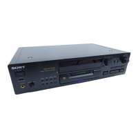
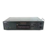
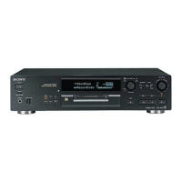
Identifies similar models and mechanism types for reference.

Self-Diagnosis Function

Error Codes and Countermeasures

Lists self-diagnosis error codes and their causes/remedies.

Error History Display Mode Procedure

Step-by-step guide for accessing the error history display mode.

Error History Mode Contents

Test Mode Selection and Error Code Table

Details on selecting test modes and a table of error codes.

Servicing Notes

Safety Check-out Procedures

Essential safety checks before customer release.

AC Leakage Test

Method for performing AC leakage testing on the unit.

Handling Optical Pick-up and Laser Diode

Optical Pick-up and Base Unit Handling Notes

Precautions for handling the optical pick-up and base unit.

Laser Diode Emission Check Safety

Safety guidelines for checking laser diode emission.

BD Board Waveform Checking Jig

Jig Setup and Terminal Identification

Details on using the jig for BD board waveform checks.

IOP Data Recording and Display

Recording IOP Values

Procedure to record optical pick-up IOP data.

Displaying Recorded IOP Values

How to read back recorded IOP data.

Forced System Reset

Reset Procedure

Instructions for performing a system microprocessor reset.

Pre-Repair Checks and Adjustments

Laser Power, Traverse, and Focus Bias Checks

Procedures for checking laser power, traverse, and focus bias.

C PLAY, Self-Recording/Playback, and Temp Compensation Checks

Checks for C PLAY, self-recording/playback, and temp compensation.

Retry Cause Display Mode

Procedure for Retry Cause Display

Steps to access and use the retry cause display.

Interpreting Retry Cause Displays

Guide to understanding retry cause codes and their meanings.

General Information

Front Panel Controls Overview

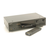
Description of front panel buttons and their functions.

Setting the Unit's Internal Clock

Instructions for setting the clock and date.

Remote Control Parts Description

Clock Setting and Display

Changing Clock Settings

Procedure for modifying existing clock settings.

Displaying Current Date and Time

Method to view the current date and time.

Disassembly Procedures

Removing the Outer Case

Steps to remove the unit's outer case.

Disassembling the Front Panel Section

Detailed steps for front panel disassembly.

Board and Mechanism Disassembly

Main Board Removal

Steps for removing the main board assembly.

Mechanism Deck Removal

Procedure to remove the mechanism deck (MDM-5D).

Mechanism Component Disassembly

Slider (Cam) Mechanism

Disassembly steps for the slider (cam) mechanism.

Base Unit and BD Board

Details on base unit and BD board disassembly.

SW Board and Loading Motor

SW Board and Loading Motor (M103) Disassembly

Steps for disassembling the SW board and loading motor.

Test Mode Operations

Precautions for Test Mode Use

Important safety warnings before entering test modes.

Entering and Setting the Test Mode

Methods for accessing and configuring test modes.

Releasing the Test Mode

Procedure to exit test mode and return to standby.

Basic Test Mode Operations

Overview of button functions within test modes.

Selecting Test Mode Functions

Test Mode Groups and Item Descriptions

Lists available test modes, their numbers, and descriptions.

Special Operating Modes

Continuous Playback Mode Operations

Steps for entering, operating, and ending continuous playback.

Continuous Recording Mode Operations

Steps for entering, operating, and ending continuous recording.

Non-Volatile Memory Mode (EEP MODE)

Functionality for reading and writing non-volatile memory.

Test Mode Displays Explained

Understanding Test Mode Displays

Explains various displays in test mode: mode, error rates, addresses, auto gain, detrack, IVR.

Display Indicator Meanings

Interpreting Unit Displays

Explains the meaning of various display indicators during operation.

Electrical Adjustments Overview

Parts Replacement and Adjustment Flowchart

Flowchart guiding adjustments after component replacement.

Adjustment Precautions and Disc Creation

Laser Emission and Optical Pick-up Precautions

Safety notes for laser emission checks and pick-up handling.

General Adjustment Precautions

Important precautions before performing adjustments.

Creating a Continuous Recording Disc

Procedure for preparing a test disc for adjustments.

Pre-Repair Checks

Temperature Compensation Offset Check

Procedure to check the temperature compensation offset.

Laser Power and Traverse Checks

Detailed checks for laser power and traverse mechanism.

Traverse Waveform Analysis

How to analyze traverse waveforms using an oscilloscope.

Specific Checks and Adjustments

Focus Bias Check Procedure

Steps to check focus bias and tolerance.

C PLAY Error Rate Checks (MO/CD)

Procedures for checking MO and CD error rates in C PLAY.

Self-Recording/Playback Check Procedure

Steps to perform a self-recording/playback error rate check.

Adjustment Procedures

Initial Setting of Adjustment Values

Resets adjustment values to their initial state.

IOP Data Recording and Display

Manages IOP data for the optical pick-up.

Temperature Compensation Offset Adjustment

Adjusts for temperature variations.

Laser Power Adjustment

Adjusts laser power output levels.

Laser Power and Traverse Adjustments

Laser Power Adjustment Procedure

Detailed steps for adjusting laser power.

Traverse Adjustment Procedure

Steps for adjusting the traverse mechanism.

Traverse and Focus Bias Adjustments

Traverse Adjustment (Write Power)

Adjusts traverse waveform for write power.

Focus Bias Adjustment Procedure

Steps to adjust focus bias based on C1 error rates.

Error Rate, Focus Bias, and Gain Adjustments

Error Rate Checks (CD/MO)

Procedures for checking CD and MO error rates.

Focus Bias Check Procedure

Checks focus bias and tolerance.

Auto Gain Control Adjustment (CD/MO)

Adjusts auto gain for CD and MO signal outputs.

Adjustment Location Diagrams

BD Board (Side A) Adjustment Points

Diagram showing adjustment locations on BD board, side A.

BD Board (Side B) Adjustment Points

Diagram showing adjustment locations on BD board, side B.

Diagrams - Servo Section

Servo Section Block Diagram

Block diagram illustrating the servo system's circuitry.

Diagrams - Main Section

Main Section Block Diagram

Block diagram illustrating the main section's circuitry.

Notes on Diagrams

Printed Wiring Board Conventions

Explains symbols and conventions for printed wiring boards.

Schematic Diagram Conventions

Explains symbols and conventions for schematic diagrams.

Circuit Board Locations

Diagram of Board Layout

Visual guide showing the location of each circuit board within the unit.

BD Board Printed Wiring

BD Board (Side A) Layout

Printed wiring layout for the BD board, side A.

BD Board (Side B) Layout

Printed wiring layout for the BD board, side B.

BD Board Schematic Diagram (1/2)

BD Board Schematic (Part 1)

Schematic diagram for the BD board, covering part 1.

BD Board Schematic Diagram (2/2)

BD Board Schematic (Part 2)

Schematic diagram for the BD board, covering part 2.

SW Board Diagrams

SW Board Schematic Diagram

Circuit diagram for the SW board.

SW Board Printed Wiring Layout

Component layout for the SW board.

MAIN and BAT Board Schematics (1/3)

MAIN Board Schematic (Part 1)

Schematic diagram for the MAIN board, part 1.

BAT Board Schematic

Circuit diagram for the BAT board.

MAIN Board Schematic Diagram (2/3)

MAIN Board Schematic (Part 2)

Schematic diagram for the MAIN board, part 2.

MAIN Board Schematic Diagram (3/3)

MAIN Board Schematic (Part 3)

Schematic diagram for the MAIN board, part 3.

MAIN Board Printed Wiring (Side A)

MAIN Board (Side A) Layout

Printed wiring layout for the MAIN board, side A.

MAIN and BAT Board Printed Wiring

MAIN Board (Side B) Layout

Printed wiring layout for the MAIN board, side B.

BAT Board Layout

Printed wiring layout for the BAT board.

AC Board Printed Wiring

AC Board (Side A) Layout

Printed wiring layout for the AC board, side A.

AC Board (Side B) Layout

Printed wiring layout for the AC board, side B.

AC Board Schematic Diagram

AC Board Circuit Diagram

Circuit diagram for the AC board.

Panel Section Printed Wiring Boards

DISP, PSW, HP Board Layouts

Printed wiring layouts for DISP, PSW, and HP boards.

KEY and VOL Board Layouts

Printed wiring layouts for KEY and VOL boards.

Panel Section Schematic Diagrams

PSW, VOL, HP, KEY, DISP Board Schematics

Circuit diagrams for PSW, VOL, HP, KEY, and DISP boards.

IC Block Diagrams

BD Board IC101 CXA2523AR Block Diagram

Block diagram for IC101 on the BD board.

IC Block Diagrams (Main Board)

IC121 CXD2656R Block Diagram

Block diagram for IC121 CXD2656R.

IC152 BH6511FS-E2 Block Diagram

Block diagram for IC152 BH6511FS-E2.

IC Block Diagrams (Main Board Continued)

IC100, IC203/204, IC300, IC400 Block Diagrams

Block diagrams for IC100, IC203/204, IC300, and IC400.

IC Block Diagrams (Main Board Continued)

IC200 CXD8735N-TP Block Diagram

Block diagram for IC200 CXD8735N-TP.

IC Block Diagrams (Main Board Continued)

IC700 LA5632 and IC701 M5293L Block Diagrams

Block diagrams for IC700 and IC701.

IC Pin Function Descriptions

BD Board IC101 CXA2523AR Pin Functions

Detailed pinout for IC101 on the BD board.

IC Pin Function Descriptions (BD Board Continued)

BD Board IC121 CXD2656R Pin Functions

Detailed pinout for IC121 CXD2656R on the BD board.

IC Pin Function Descriptions (BD Board Continued)

BD Board IC121 CXD2656R Pin Functions (Continued)

Continued detailed pinout for IC121 CXD2656R.

IC Pin Function Descriptions (BD Board Continued)

BD Board IC121 CXD2656R Pin Functions (Final)

Final detailed pinout for IC121 CXD2656R.

Main Board IC800 Pin Functions

IC800 System Controller Pin Functions

Detailed pinout for IC800, the system controller.

Main Board IC800 Pin Functions (Continued)

IC800 Pin Functions (Continued)

Continued pinout details for IC800.

Main Board IC800 Pin Functions (Continued)

IC800 Pin Functions (Final)

Final pinout details for IC800, including motor control.

Exploded Views - Chassis Section

Chassis Section Exploded View

Exploded diagram of the chassis section and its components.

Exploded Views - Front Panel Section

Front Panel Components Exploded View

Exploded diagram of front panel components.

Exploded Views - Mechanism Section (MDM-5D)

Mechanism Section (MDM-5D) Exploded View

Exploded diagram of the mechanism section (MDM-5D).

Exploded Views - Base Unit Section (MBU-5D)

Base Unit Section (MBU-5D) Exploded View

Exploded diagram of the base unit section (MBU-5D).

Electrical Parts List

Component Lists (Resistors, Capacitors, Diodes, ICs, etc.)

Comprehensive list of electronic components with part numbers.

BD Board Parts List

BD and Display Board Parts Lists

DISP, HP, KEY, and MAIN Board Parts Lists

DISP, HP, KEY, MAIN Board Components (Resistors, Capacitors, Switches, etc.)

Component lists for DISP, HP, KEY, and MAIN boards.

MAIN Board Parts List (Capacitors, Connectors, Diodes, ICs, Resistors)

MAIN Board Capacitors and Connectors

Detailed lists of capacitors and connectors for the MAIN board.

MAIN Board Parts List (Connectors, Diodes, ICs)

MAIN Board Connectors, Diodes, and ICs

Detailed lists of connectors, diodes, and ICs for the MAIN board.

MAIN Board Parts List (Resistors, Transistors)

MAIN Board Resistors and Transistors

Detailed lists of resistors and transistors for the MAIN board.

MAIN Board Parts List (Resistors)

MAIN Board Resistors (Continued)

Continuation of the resistor list for the MAIN board.

MAIN, PSW, SW, VOL Board Parts Lists

MAIN, PSW, SW, VOL Board Components (Switches, Connectors, Capacitors, etc.)

Detailed component lists for MAIN, PSW, SW, and VOL boards.

Hardware, Accessories, and Packing Materials

Hardware List

List of screws and hardware used in the unit.

Accessories and Packing Materials

List of included accessories and packing items.
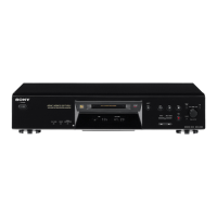
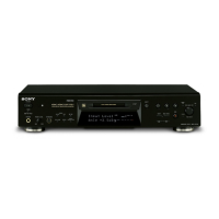
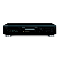
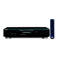
Related product manuals