EasyManua.ls Logo

Sony MDS-JE530 Service Manual

Sony MDS-JE530
64 pages
To Next Page IconTo Next Page
Page #1 background imageLoading...
Page #1 background image
MICROFILM
SERVICE MANUAL
MINI DISC DECK
US Model
Canadian Model
AEP Model
UK Model
E Model
SPECIFICATIONS
MDS-JE530
Model Name Using Similar Mechanism MDS-JE520
MD Mechanism Type MDM-5D
Optical Pick-up Type KMS-260B/J1N
U.S. and foreign patents licensed form Dolby Laboratories
Licensing Corporation.
Photo: Black model
System MiniDisc digital audio system
Disc MiniDisc
Laser Semiconductor laser (λ = 780 nm)
Emission duration: continuous
Laser output Less than 44.6 µW*
* This output is the value measured
at a distance of 200 mm from the
objective lens surface on the Optical
Pick-up Block with 7 mm aperture.
Laser diode Material: GaAlAs
Revolutions (CLV) 400 rpm to 900 rpm
Error correction Advanced Cross Interleave Reed
Solomon Code (ACIRC)
Sampling frequency 44.1 kHz
Coding Adaptive Transform Acoustic Coding
(ATRAC)
Modulation system EFM (Eight-to-Fourteen Modulation)
Number of channels 2 stereo channels
Frequency response 5 to 20,000 Hz ±0.3 dB
Signal-to-noise ratio Over 98 dB during playback
Wow and flutter Below measurable limit
Input
LINE (ANALOG) IN Jack type: phono
Impedance: 47 kilohms
Rated input: 500 mVrms
Minimum input: 125 mVrms
DIGITAL OPTICAL IN Connector type: square optical
Impedance: 600 nm (optical wave length)
DIGITAL COAXIAL IN Jack type: phono
Impedance: 75 ohms
Rated input: 0.5 Vp-p, ±20%
Outputs
PHONES Jack type: stereo phone
Rated output: 28 mW
Load impedance: 32 ohms
LINE (ANALOG) OUT Jack type: phono
Rated output: 2 Vrms (at 50 kilohms)
Load impedance: Over 10 kilohms
DIGITAL OPTICAL OUT Connector type: square optical
Rated output: –18 dBm
Load impedance: 660 nm (optical
wave length)
General
Power requirements
North American model: 120 V AC, 60 Hz
European model: 230 V AC, 50/60 Hz
Other models: 110 – 120 V or 220 – 240 V AC, 50/60 Hz
Adjustable with voltage selector
Power consumption 16 W
Dimension (approx.) 430 × 95 × 280 mm (w/h/d) incl.
projecting parts and controls
Mass (approx.) 3.4 kg
Supplied accessories
Audio connecting cords (2)
• Optical cable (1)
• Remote commander (remote) RM-D29M (1)
• R6 (size-AA) batteries (2)

Other manuals for Sony MDS-JE530

Question and Answer IconNeed help?

Do you have a question about the Sony MDS-JE530 and is the answer not in the manual?

Sony MDS-JE530 Specifications

General IconGeneral
BrandSony
ModelMDS-JE530
CategoryMiniDisc Player
LanguageEnglish

Summary

SPECIFICATIONS

System Specifications

Details of device system, disc, laser, and signals.

Input and Output Specifications

Details of analog and digital input/output connectors and levels.

General Specifications and Accessories

Covers power, dimensions, mass, and included accessories.

SELF-DIAGNOSIS FUNCTION

Error Code Causes and Remedies

Lists three-digit error codes, their causes, and suggested countermeasures.

Error History Display Mode Procedure

Step-by-step guide to entering and using the error history display mode.

ERROR HISTORY MODE ITEMS AND CONTENTS

Test Mode Selection and History Displays

Explains various test mode displays and how to select them.

Error Code Details

Provides a table detailing specific error codes and their meanings.

SECTION 1 SERVICING NOTES

Safety Check-out Procedures

Instructions for performing safety checks before releasing the unit to the customer.

Leakage Test Procedure

Details the method and limits for testing AC leakage current.

SAFETY PRECAUTIONS AND REPAIR GUIDELINES

Battery Handling and Laser Safety Warnings

Warnings about battery replacement and laser emission hazards.

Circuit Board and Component Repair Notes

Guidance on flexible circuit board repair and chip component replacement.

Safety-Related Component Warning

Highlights components critical to safe operation and replacement advice.

JIG FOR CHECKING BD BOARD WAVEFORM

Jig Specifications and Terminal Names

Describes the jig for checking BD board waveforms and its terminal definitions.

IOP DATA RECORDING AND DISPLAY

IOP Value Recording Procedure

Steps for recording the IOP value onto the non-volatile memory.

IOP Value Display Procedure

Steps for reading the recorded IOP value from the non-volatile memory.

CHECKS PRIOR TO PARTS REPLACEMENT AND ADJUSTMENTS

Determination Criteria for Key Checks

Lists criteria for determining component satisfaction before replacement.

Unsatisfactory Measurement Procedures

Outlines what to measure if components do not meet criteria.

RETRY CAUSE DISPLAY MODE

Entering the Retry Cause Display Mode

Procedure to enter the test mode for viewing retry causes.

Reading Retry Cause Display Data

Explains how to interpret the displayed retry cause hexadecimal data.

RETRY CAUSE DISPLAY DATA INTERPRETATION

Interpreting Retry Cause Hexadecimal Values

Details how to convert hex to binary to understand retry causes.

Hexadecimal to Binary Conversion Table

Provides a reference table for converting hex digits to binary.

SECTION 2 GENERAL

Location of Controls

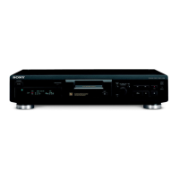
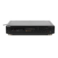
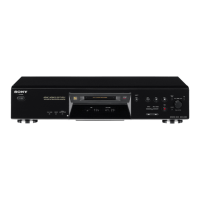
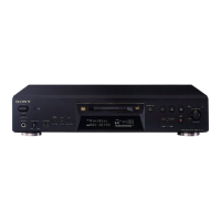
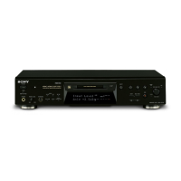
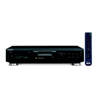
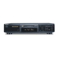
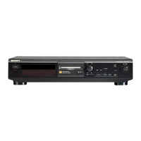
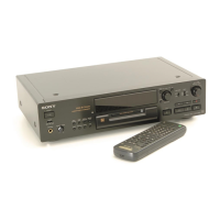
Identifies and describes the function of each control on the unit.

REMOTE PARTS DESCRIPTIONS

Remote Control Button Functions

Explains the function of each button on the remote commander.

SECTION 3 DISASSEMBLY

Case Disassembly Procedure

Steps for removing the outer case of the unit.

Front Panel Section Disassembly

Procedure for removing the front panel section.

BOARD AND MECHANISM DISASSEMBLY

Main Board Removal Procedure

Steps for removing the main board and its connectors.

Mechanism Deck (MDM-5D) Removal

Procedure for detaching the MD mechanism deck.

MECHANISM COMPONENT DISASSEMBLY

Slider (Cam) Component Removal

Steps for disassembling the slider (cam) mechanism.

Base Unit and BD Board Disassembly

Procedure for disassembling the base unit and BD board.

SUB-ASSEMBLY DISASSEMBLY

SW Board and Loading Motor Removal

Steps for removing the SW board and loading motor.

SECTION 4 TEST MODE

Precautions for Test Mode Use

Important notes and precautions before entering test modes.

Setting and Exiting Test Modes

Procedures for entering, navigating, and exiting various test modes.

SELECTING TEST MODES

Test Mode Group Selection

Explains how to select test mode groups for servicing or development.

Specific Test Mode Descriptions

Lists and briefly describes various test modes, e.g., TEMP CHECK, LDPWR CHECK.

OPERATING CONTINUOUS MODES

Continuous Playback Mode Operation

How to enter and operate the continuous playback mode.

Continuous Recording Mode Operation

How to enter and operate the continuous recording mode for checks.

Non-Volatile Memory Mode (EEP MODE)

Describes the EEP MODE and its purpose.

FUNCTIONS OF OTHER BUTTONS AND TEST MODE DISPLAYS

Other Button Functions

Explains the functions of various operational buttons not covered elsewhere.

Test Mode Display Sequences

Describes how displays change when the DISPLAY/CHAR button is pressed in test mode.

MEANINGS OF OTHER DISPLAYS

Display Indicators and Their Meanings

Explains various display indicators when lit or off during operation.

SECTION 5 ELECTRICAL ADJUSTMENTS

Parts Replacement and Adjustment Flowchart

Outlines the procedure for parts replacement and subsequent adjustments.

Adjustment Procedures Overview

Lists key adjustments like temperature compensation and laser power.

PRECAUTIONS FOR ADJUSTMENTS AND CONTINUOUS RECORDING DISC CREATION

Adjustment Precautions and Tool Usage

General precautions for adjustments and required tools/devices.

Creating a Continuous Recording Disc

Steps to create a specific disc needed for focus bias and error rate checks.

CHECK PRIOR TO REPAIRS

Temperature Compensation Offset Check

Procedure to check temperature compensation offset.

Laser Power Check Procedure

Steps for checking the optical pick-up's laser power output.

Traverse Check Procedure

How to perform a traverse check using an oscilloscope.

FOCUS BIAS AND PLAYBACK CHECKS

Traverse Check Waveform Specifications

Specifies waveform values for traverse checks.

Focus Bias Check Procedure

Steps to check focus bias and tolerance.

C PLAY and CD Error Rate Checks

Procedures for checking C PLAY and CD error rates.

Self-Recording/Playback Check

How to perform a self-recording/playback check.

INITIAL SETTING AND LASER POWER ADJUSTMENT

Initial Setting of Adjustment Value

Procedure to reset adjustment results to initial values.

Laser Power Adjustment Procedure

Steps to adjust the laser power output using a power meter.

LASER POWER AND TRAVERSE ADJUSTMENT

Laser Power Check and IOP Information Recording

Further laser power checks and IOP value recording.

Traverse Adjustment Procedure

Steps to adjust traverse waveforms for MO and CD.

TRAVERSE AND FOCUS BIAS ADJUSTMENTS

Traverse Adjustment Waveform Specifications

Specifies waveform values for traverse adjustments.

Focus Bias Adjustment Procedure

Steps to adjust focus bias based on C1 error rate.

ERROR RATE CHECKS AND AUTO GAIN ADJUSTMENT

CD and MO Error Rate Checks

Procedures for checking CD and MO error rates.

Focus Bias Check

Re-checks focus bias after adjustments.

Auto Gain Control Output Level Adjustment

Steps to adjust auto gain levels for CD and MO.

BD BOARD ADJUSTMENT LOCATIONS

BD Board Component Layout

Diagrams showing component locations on BD Board Sides A and B.

SECTION 6 DIAGRAMS

Block Diagram - MD SERVO Section

High-level block diagram of the MD servo system.

BLOCK DIAGRAM - MAIN SECTION

Analog and Digital Signal Paths

Block diagram showing signal flow in the main section, including A/D, D/A conversion.

NOTES FOR PRINTED WIRING BOARDS AND SCHEMATIC DIAGRAMS

Printed Wiring Board Notation Guide

Explains symbols and notations used on printed wiring boards.

Schematic Diagram Notation Guide

Explains symbols and notations used in schematic diagrams.

CIRCUIT BOARDS LOCATION

Diagram of Board Locations

Illustrates the physical placement of various circuit boards within the unit.

PRINTED WIRING BOARD - BD BOARD

BD Board (Side A) Component Layout

Shows component placement on the BD board, Side A.

BD Board (Side B) Component Layout

Shows component placement on the BD board, Side B.

SCHEMATIC DIAGRAM - BD BOARD (1/2)

BD Board Circuit Diagram

Part 1 of the BD board schematic, detailing its circuitry.

SCHEMATIC DIAGRAM - BD BOARD (2/2)

BD Board Circuit Diagram Continued

Part 2 of the BD board schematic, continuing its circuitry.

WAVEFORMS

BD Board Waveform Examples

Illustrates typical waveforms measured on the BD board at specific points.

Main and Display Board Waveforms

Shows waveform examples from the Main and Display boards.

PRINTED WIRING BOARD - MAIN BOARD

Main Board Component Layout

Shows component placement on the main board.

SCHEMATIC DIAGRAM - MAIN BOARD (1/2)

Main Board Circuit Diagram

Part 1 of the main board schematic, detailing its circuitry.

SCHEMATIC DIAGRAM - MAIN BOARD (2/2)

Main Board Circuit Diagram Continued

Part 2 of the main board schematic, continuing its circuitry.

PRINTED WIRING BOARDS - PANEL SECTION

Display Board Component Layout

Shows component placement on the display board.

Key Switch Board Component Layout

Shows component placement on the key switch board.

Power Switch and HP Boards Component Layout

Shows component placement on power switch and HP boards.

SCHEMATIC DIAGRAM - PANEL SECTION

Display, Power SW, and Key SW Board Schematics

Circuit diagrams for the display, power switch, and key switch boards.

IC BLOCK DIAGRAMS

IC101 CXA2523AR Block Diagram

Internal block diagram of the CXA2523AR IC.

IC121 CXD2656R Block Diagram

Internal block diagram of the CXD2656R IC.

IC152 BH6511FS Block Diagram

Internal block diagram of the BH6511FS IC.

IC BLOCK DIAGRAMS (MAIN BOARD)

IC310 M5293L Block Diagram

Internal block diagram of the M5293L IC.

IC321 AK4524 Block Diagram

Internal block diagram of the AK4524 IC.

IC431 LA5632 Block Diagram

Internal block diagram of the LA5632 IC.

IC471 LB1641 Block Diagram

Internal block diagram of the LB1641 IC.

IC PIN FUNCTION DESCRIPTION - BD BOARD

IC101 CXA2523AR Pin Functions

Detailed pin functions for IC101 CXA2523AR on the BD board.

IC PIN FUNCTION DESCRIPTION - BD BOARD (Cont.)

IC121 CXD2656R Pin Functions

Detailed pin functions for IC121 CXD2656R on the BD board.

IC PIN FUNCTION DESCRIPTION - BD BOARD (Cont.)

IC121 CXD2656R Pin Functions

Continues detailed pin functions for IC121 CXD2656R on the BD board.

IC PIN FUNCTION DESCRIPTION - BD BOARD (Cont.)

IC121 CXD2656R Pin Functions

Concludes detailed pin functions for IC121 CXD2656R on the BD board.

IC PIN FUNCTION DESCRIPTION - MAIN BOARD

IC501 M30624MG-207FP Pin Functions

Detailed pin functions for IC501 M30624MG-207FP on the main board.

IC PIN FUNCTION DESCRIPTION - MAIN BOARD (Cont.)

IC501 M30624MG-207FP Pin Functions

Continues detailed pin functions for IC501 M30624MG-207FP on the main board.

IC PIN FUNCTION DESCRIPTION - MAIN BOARD (Cont.)

IC501 M30624MG-207FP Pin Functions

Concludes detailed pin functions for IC501 M30624MG-207FP on the main board.

SECTION 7 EXPLODED VIEWS

Chassis Section Exploded View

Exploded view of the chassis section with part identification.

FRONT PANEL SECTION EXPLODED VIEW

Front Panel Assembly Exploded View

Exploded view of the front panel section with part identification.

MECHANISM SECTION (MDM-5D) EXPLODED VIEW

MD Mechanism Section Exploded View

Exploded view of the MD mechanism section (MDM-5D).

BASE UNIT SECTION (MBU-5D) EXPLODED VIEW

Base Unit Section Exploded View

Exploded view of the base unit section (MBU-5D).

SECTION 8 ELECTRICAL PARTS LIST

BD Board Capacitors and Diodes

Lists capacitors and diodes for the BD board.

BD Board ICs and Transistors

Lists ICs and transistors for the BD board.

BD DISPLAY PARTS LIST

BD Display Coils, Transistors, and Resistors

Lists coils, transistors, and resistors for the BD display.

BD Display Switches and Capacitors

Lists switches and capacitors for the BD display.

DISPLAY, HP, KEY SW PARTS LIST

Display Board Components

Lists components for the display board.

HP and Key SW Board Components

Lists components for the HP and Key SW boards.

MAIN BOARD PARTS LIST

Main Board ICs and Connectors

Lists ICs and connectors for the main board.

Main Board Coils and Diodes

Lists coils and diodes for the main board.

MAIN BOARD PARTS LIST (Cont.)

Main Board ICs and Transistors

Lists ICs and transistors for the main board.

Main Board Resistors and Ground Plate

Lists resistors and ground plate for the main board.

MAIN BOARD PARTS LIST (Cont.)

Main Board Resistors

Lists various resistors for the main board.

MAIN POWER SW BOARD AND MISCELLANEOUS PARTS

Main Power SW Board Components

Lists components for the main power SW board.

Miscellaneous Hardware and Accessories

Lists hardware, accessories, and packing materials.

Related product manuals