EasyManua.ls Logo

Sony MDS-JE480 Service Manual

Sony MDS-JE480
68 pages
To Next Page IconTo Next Page
Page #1 background imageLoading...
Page #1 background image
MDS-JE480
SPECIFICATIONS
SERVICE MANUAL
MINIDISC DECK
Model Name Using Similar Mechanism MDS-JE470
MD Mechanism Type MDM-7S1A
Optical Pick-up Type KMS-260B/260E
US Model
AEP Model
UK Model
US and foreign patents licensed form Dolby Laboratories
Licensing Corporation.
9-873-964-05
2006B02-1
© 2006.02
Sony Corporation
Home Audio Division
Published by Sony Techno Create Corporation
Ver. 1.4 2006.02
System MiniDisc digital audio system
Disc MiniDisc
Laser Semiconductor laser
(λ = 780 nm) Emission
duration: continuous
Laser output MAX 44.6 µW
1)
1) This output is the value measured at a distance of
200mm from the objective lens surface on the
Optical Pick-up Block with 7 mm aperture.
Laser diode Material: GaAlAs
Revolutions (CLV) 400 rpm to 900 rpm
Error correction ACIRC (Advanced Cross
Interleave Reed Solomon Code)
Sampling frequency 44.1 kHz
Coding ATRAC (Adaptive
Transform Acoustic Coding)/
ATRAC 3
Modulation system EFM (Eight-to-Fourteen
Modulation)
Number of channels 2 stereo channels
Frequency response 5 to 20,000 Hz ±0.5 dB
during play
Signal-to-noise ratio Over 96 dB during play
Wow and flutter Below measurable limit
Inputs
ANALOG IN Jack type: phono
Impedance: 47 kilohms
Rated input: 500 mVrms
Minimum input: 125 mVrms
DIGITAL OPTICAL IN Connector type: square optical
Impedance: 660 nm
(optical wave length)
Outputs
ANALOG OUT Jack type: phono
Rated output: 2 Vrms (at 50 kilohms)
Load impedance: over 10 kilohms
General
Power requirements
US model: 120 V AC, 60Hz
European model: 230 V AC, 50/60Hz
Power consumption 14 W (0.5 W in standby mode)
Dimensions (approx.) 430 x 95 x 285 mm
(w/h/d) incl. projecting
parts and controls
Mass (approx.) 3.0 kg
Supplied accessories
Audio connecting cords (2)
Optical cable (1)
Remote commander (remote) (1)
R6 (size-AA) batteries (2)
Design and specifications are subject to change without notice.
w
w
w
.
x
i
a
o
y
u
1
6
3
.
c
o
m
Q
Q
3
7
6
3
1
5
1
5
0
9
9
2
8
9
4
2
9
8
T
E
L
1
3
9
4
2
2
9
6
5
1
3
9
9
2
8
9
4
2
9
8
0
5
1
5
1
3
6
7
3
Q
Q
TEL 13942296513 QQ 376315150 892498299
http://www.xiaoyu163.com

Other manuals for Sony MDS-JE480

Question and Answer IconNeed help?

Do you have a question about the Sony MDS-JE480 and is the answer not in the manual?

Sony MDS-JE480 Specifications

General IconGeneral
MaterialPlastic
I/O ports1 x Opt. - in
Device typeHiFi minidisc player
Frequency range5 - 20000 Hz
Shock resistant memory10 s
Audio A/D Converter (ADC)24 bit
Signal-to-Noise Ratio (SNR)96 dB
Product colorSilver
Power requirements230 V; 50/60 Hz
Power consumption (standby)0.5 W
Power consumption (typical)15 W
Weight and Dimensions IconWeight and Dimensions
Weight3000 g
Dimensions (WxDxH)430 x 285 x 95 mm

Summary

SERVICE MANUAL

SPECIFICATIONS

Detailed technical specifications of the MD deck.

Digital Optical Input Specifications

Technical specifications for the digital optical input.

Analog Output Specifications

Technical specifications for the analog output.

General Specifications

General specifications including power and dimensions.

SAFETY CHECK-OUT

AC Leakage Check

Procedure for checking AC leakage from metal parts.

Optical Pick-up Handling Precautions

Precautions for handling the optical pick-up block.

Laser Diode Emission Safety

Safety warning regarding laser diode emission checks.

Adjustment and Component Safety Warnings

Warnings about incorrect adjustments and component replacement.

SELF-DIAGNOSIS FUNCTION

Using Self-Diagnosis Function

Steps to use the self-diagnosis function in error history mode.

ERROR HISTORY MODE ITEMS

Selecting Test Mode Items

How to select different items for error history display.

MODEL IDENTIFICATION

SERVICE NOTES

Jig for BD Board Waveform Check

Description and use of a special jig for checking BD board waveforms.

Iop Data Recording and Display

Record Procedure

Steps to record Iop value into non-volatile memory.

Display Procedure

Steps to display recorded Iop value from non-volatile memory.

Optical Pick-up Block Type Discrimination

Checks Prior to Parts Replacement and Adjustments

Forced Reset Procedure

Procedure for forcing a system microprocessor reset.

Retry Cause Display Mode

Procedure for Retry Cause Display

Steps to enter and use the retry cause display mode.

Interpreting Retry Cause Display

How to interpret the retry cause display data.

Track Mode Display Interpretation

GENERAL

Main Unit Overview

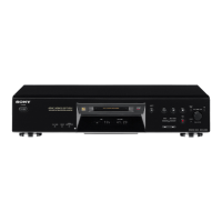
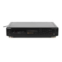
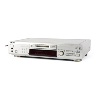
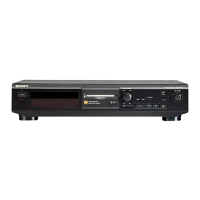
Overview of the main unit with labeled controls and indicators.

Button Descriptions

Description of the function for each button.

DISASSEMBLY

Disassembly Flow

Flowchart outlining the disassembly sequence.

Disassembly Steps

Upper Case Removal

Instructions for removing the upper case.

Front Panel Section Disassembly

Instructions for disassembling the front panel section.

Board Removal Procedures

Main Board Removal

Instructions for removing the main board.

PT Board Removal

Instructions for removing the PT board.

Component Removal Procedures

Mechanism Deck Removal

Instructions for removing the mechanism deck.

Over Light Head and BD Board Removal

Instructions for removing the over light head and BD board.

Component Removal Procedures

Holder Assy Disassembly

Instructions for disassembling the holder assembly.

Loading Motor Assy Removal

Instructions for removing the loading motor assembly.

Component Removal Procedures

Sled Motor Assy and Slider Removal

Instructions for removing the sled motor assembly and slider.

Optical Pick-up Removal

Instructions for removing the optical pick-up.

Component Removal Procedures

Spindle Motor Assy Removal

Instructions for removing the spindle motor assembly.

TEST MODE Operations

Precautions for Test Mode Use

Precautions before operating the test mode.

Setting and Exiting Test Mode

Methods for entering and exiting the test mode.

Test Mode Button Operations

Functions of buttons used in test mode operations.

Selecting Test Modes

Continuous Playback and Recording Modes

Continuous Playback Mode

How to operate continuous playback mode.

Continuous Recording Mode

How to operate continuous recording mode for self-check.

Test Mode Displays

Mode Display Interpretation

Displays indicating the current test mode.

Error Rate Display Interpretation

How the error rate is displayed, including C and AD values.

Address Display Interpretation

How track and sector addresses are displayed.

Display Meanings and Self-Diagnosis

Other Display Meanings

Interpretation of various display indicators.

Automatic Self-Diagnosis Function

Performing automatic self-diagnosis for optical pick-up check.

Memory NG Handling

Procedure for handling nonvolatile memory errors.

ELECTRICAL ADJUSTMENTS

Parts Replacement and Adjustment Overview

Flowchart for checking before replacing optical pick-up parts.

Adjustment Flow

Adjustment Precautions

Laser Diode Emission Precautions

Safety warning for checking laser diode emission.

Optical Pick-up Handling Precautions

Precautions for handling optical pick-ups due to static sensitivity.

General Adjustment Precautions

General precautions before performing electrical adjustments.

Pre-Repair Checks and Procedures

Using Continuously Recorded Disc

How to create and use a continuous recorded disc for checks.

Temperature Compensation Offset Check

Checking temperature compensation offset.

Laser Power Check

Procedure for checking laser power output.

Iop Compare Check

Comparing current Iop value with non-volatile memory.

Optical Pick-up Checks

Auto Check Procedure

Performing automatic checks on optical pick-up characteristics.

Traverse Check

Checking traverse function using oscilloscope.

Focus Bias and Error Rate Checks

Focus Bias Check

Checking focus bias and tolerance.

C PLAY Error Rate Checks

Checking MO and CD error rates during playback.

Self-Recording/playback Check

Checking error rate during self-recording and playback.

Initial Setting and Iop Information

Initial Setting of Adjustment Value

Setting adjustment results to initial values.

Recording and Displaying Iop Information

Steps to record and display Iop information.

Temperature Compensation Offset Adjustment

Adjusting temperature compensation offset.

Laser Power Adjustment

Procedure for adjusting laser power.

Traverse and Iop NV Save

Traverse Adjustment

Adjusting the traverse mechanism.

Iop NV Save

Saving Iop values to non-volatile memory.

Focus Bias Adjustment

Error Rate and Gain Control Adjustments

CD Error Rate Check

Checking CD error rate.

MO Error Rate Check

Checking MO error rate.

Focus Bias Check

Checking focus bias.

Auto Gain Control Output Level Adjustment

Adjusting auto gain control output level for CD and MO.

Adjustment and Connection Points

DIAGRAMS

Circuit Boards Location

Diagram showing the location of various circuit boards.

Waveforms

Block Diagrams

BD Section Block Diagram

Block diagram of the BD section of the main unit.

Main Section Block Diagram

Printed Wiring Boards

BD Board Printed Wiring

Printed wiring board layout for the BD board.

Schematic Diagrams

BD Section Schematic (1/2)

Schematic diagram for the BD section (part 1 of 2).

BD Board Schematic

Main Section Schematic

Main Section Schematic (1/2)

Schematic diagram for the main section (part 1 of 2).

Main Section Schematic

Main Section Schematic (2/2)

Schematic diagram for the main section (part 2 of 2).

Printed Wiring Boards

Main Section Printed Wiring

Printed wiring board layout for the main section.

Printed Wiring Boards

Display Section Printed Wiring

Printed wiring board layout for the display section.

Display Section Schematic

Power Section Diagrams

Power Section Printed Wiring

Printed wiring board layout for the power section.

Power Section Schematic

Schematic diagram for the power section.

IC Pin Function Descriptions

IC101 RF Amplifier Pin Functions

Pin function description for IC101 on the BD board.

IC Pin Function Descriptions

IC201 Digital Signal Processor Pin Functions

Pin function description for IC201 on the BD board.

IC Pin Function Descriptions

IC201 Digital Signal Processor Pin Functions

Pin function description for IC201 on the BD board (continued).

IC Pin Function Descriptions

IC201 Digital Signal Processor Pin Functions

Pin function description for IC201 on the BD board (continued).

IC Pin Function Descriptions

IC1 System Control Pin Functions

Pin function description for IC1 on the main board.

IC Pin Function Descriptions

IC1 System Control Pin Functions

Pin function description for IC1 on the main board (continued).

IC BLOCK DIAGRAMS

IC101 Block Diagram

Block diagram for IC101 on the BD board.

IC Block Diagrams

IC201 Block Diagram

Block diagram for IC201 on the BD board.

IC401 Block Diagram

Block diagram for IC401 on the BD board.

IC Block Diagrams

IC803 Block Diagram

Block diagram for IC803 on the BD board.

IC440 Block Diagram

Block diagram for IC440 on the main board.

IC500 Block Diagram

Block diagram for IC500 on the main board.

EXPLODED VIEWS

Chassis Section Exploded View

Exploded view of the chassis section.

Exploded Views

Front Panel Section Exploded View

Exploded view of the front panel section.

Exploded Views

Mechanism Section-1 Exploded View

Exploded view of the mechanism section (part 1).

Exploded Views

Mechanism Section-2 Exploded View

Exploded view of the mechanism section (part 2).

ELECTRICAL PARTS LIST

Capacitors, Coils, Semiconductors, Connectors

Lists capacitors, coils, semiconductors, and connectors.

Electrical Parts List

Diodes, ICs, Transistors, Resistors

Lists diodes, ICs, transistors, and resistors.

Electrical Parts List

Switches and Lithium Battery

Lists switches and lithium battery parts.

Electrical Parts List

Ferrite Beads

Lists ferrite bead parts.

Electrical Parts List

Jacks

Lists jack parts.

ACCESSORIES

REVISION HISTORY

Related product manuals