12
NW-E403/E405/E407
SECTION 4
DIAGRAMS
Note on Schematic Diagram:
• All capacitors are in µF unless otherwise noted. (p: pF) 50 WV
or less are not indicated except for electrolytics and tantalums.
• All resistors are in Ω and
1
/
4
W or less unless otherwise speci-
fied.
•%: indicates tolerance.
• C : panel designation.
• : B+ Line.
•Voltages and waveforms are dc with respect to ground under
no-signal (detuned) conditions.
no mark : PLAY
*
: Impossible to measure
•Voltages are taken with a VOM (Input impedance 10 MΩ).
Voltage variations may be noted due to normal production toler-
ances.
•Waveforms are taken with a oscilloscope.
Voltage variations may be noted due to normal production toler-
ances.
• Circled numbers refer to waveforms.
• Signal path.
E : PLAY BACK
a : DIGITAL OUT
k : DIGITAL IN
F : AUDIO
Note on Printed Wiring Board
• X : parts extracted from the component side.
• Y : parts extracted from the conductor side.
• : Pattern from the side which enables seeing.
Caution:
Pattern face side: Parts on the pattern face side seen from
(Side A) the pattern face are indicated.
Parts face side: Parts on the parts face side seen from
(Side B) the parts face are indicated.
• MAIN board is multi-layer printed board.
However, the patterns of intermediate-layer have not been in-
cluded in the diagram.
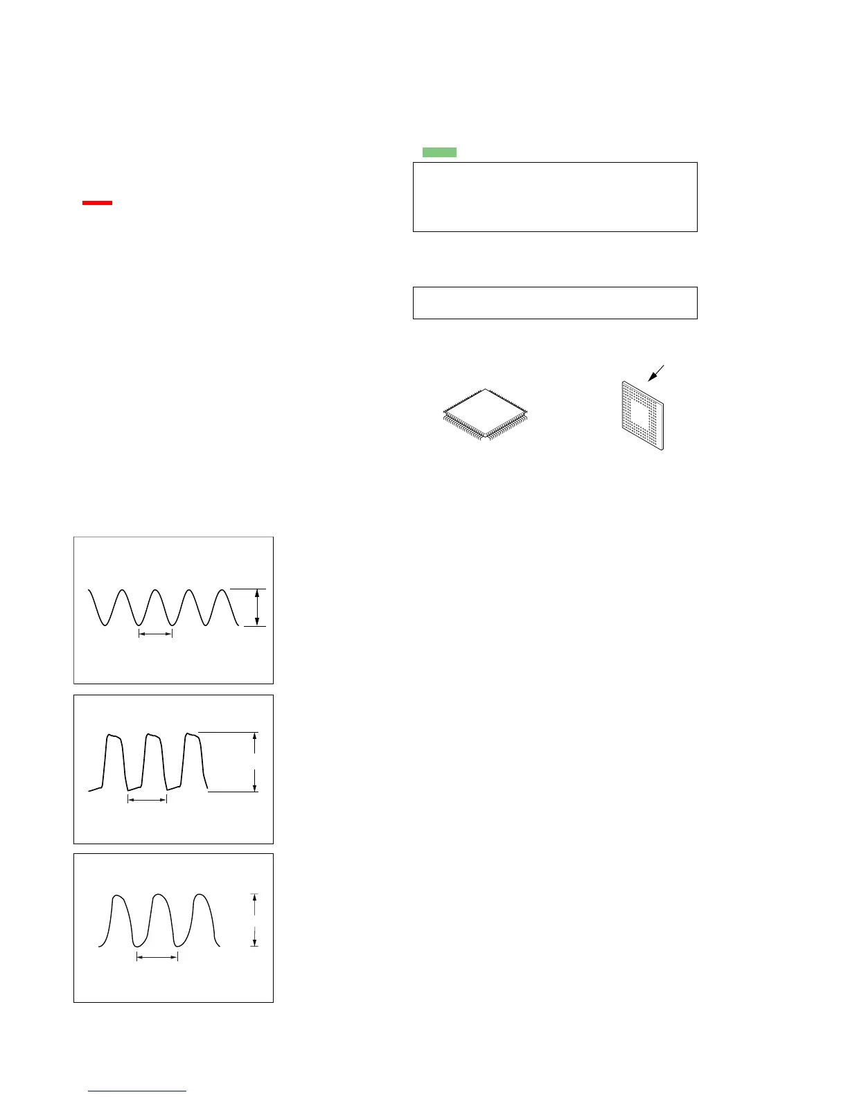
*
Replacement of IC400 on MAIN board requires a special
tool.
• Lead Layouts