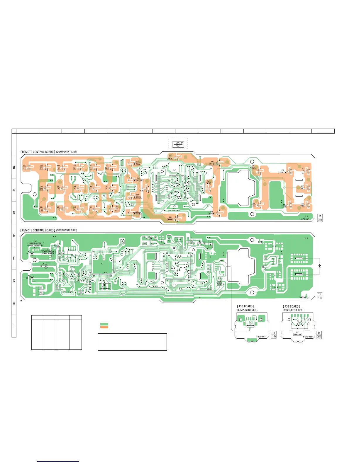
Note on Printed Wiring Boards:
• Y : parts extracted from the conductor side.
•
z
: Through hole.
•
f
: internal component.
• : Pattern from the side which enables seeing.
• : Carbon pattern.
(The other layers' patterns are not indicated.)
Caution:
Pattern face side: Parts on the pattern face side seen from
(Conductor Side) the pattern face are indicated.
Parts face side: Parts on the parts face side seen from
(Component Side) the parts face are indicated.
IC2 G-8
IC3 F-3
IC4 G-3
IC5 F-12
IC6 G-4
IC7 G-4
IC8 E-9
Q1 E-2
Q2 E-6
Ref. No. Location
Ref. No. Location
D1 F-2
D2 F-11
D3 G-1
D4 F-1
D5 C-8
D6 C-7
D7 C-8
D8 C-7
IC1 F-4
• Semiconductor Location
 Loading...