– 35 –
4-4. IC PIN FUNCTION DESCRIPTION
• MAIN BOARD IC1 µPD780058GK-A04-9EU (SYSTEM CONTROLLER)
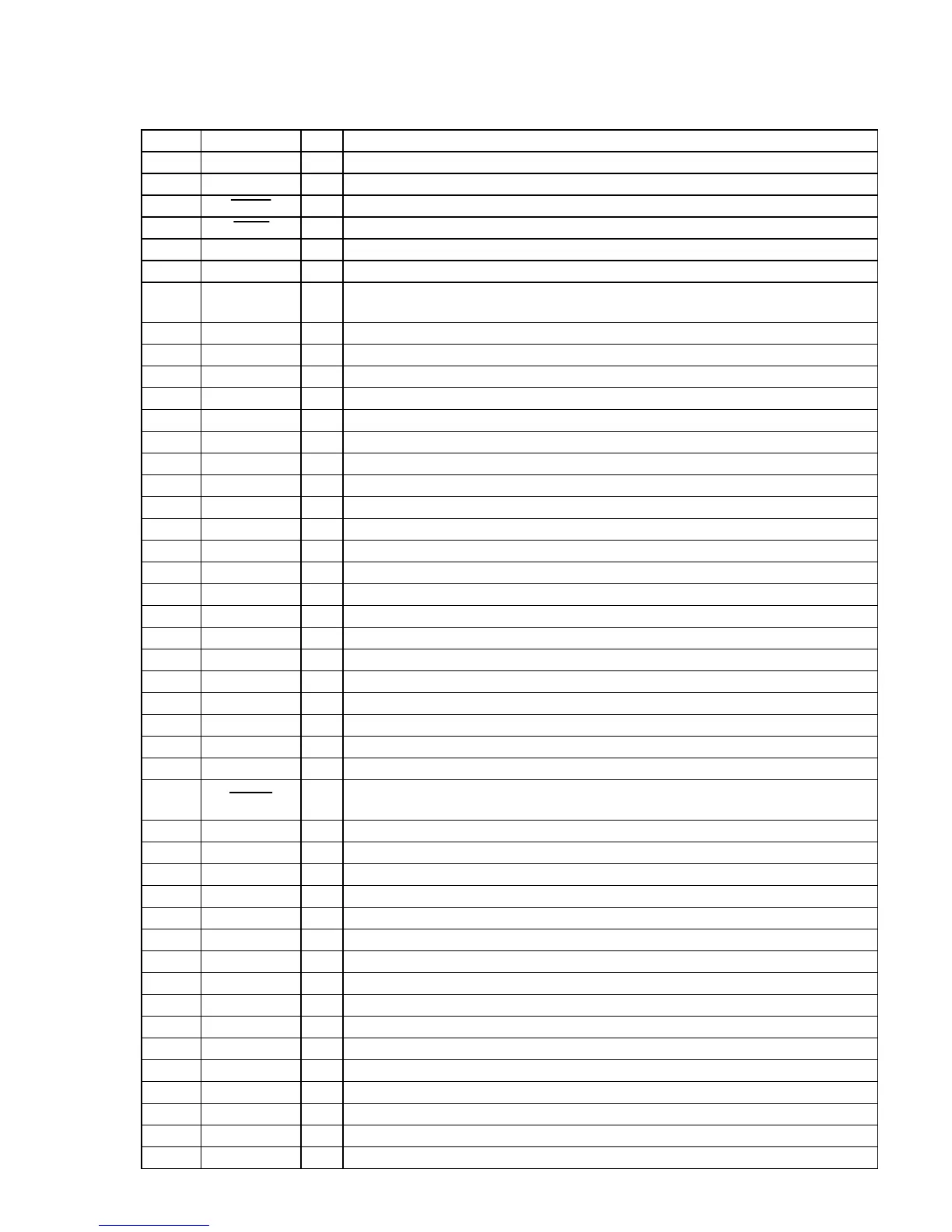
Pin No. Pin Name I/O Description
1 to 3 DB5 to DB7 I/O
Two-way data bus with the liquid crystal display driver (IC2)
4 AVSS —
Ground terminal (for A/D converter)
5 LPOW O
Power on/off control signal output for the liquid crystal display driver (IC2) “L”: power on
6 LRST O
Reset signal output to the liquid crystal display driver (IC2) “L”: reset
7 AVREF1 I
Reference voltage input terminal (for A/D converter)
8RSO
Register selection signal output to the liquid crystal display driver (IC2)
9RWO
Data read/write selection signal output to the liquid crystal display driver (IC2)
“L”: data write, “H”: data read
10 E O
Data enable signal output to the liquid crystal display driver (IC2)
11 to 15 P20 to P24 —
Not used (open)
16 SDA I/O
Two-way data bus with the EEPROM (IC3)
17 P26 —
Not used (open)
18 SCL O
Serial data transfer clock signal output to the EEPROM (IC2)
19 to 25 KDT1 to KDT7 I
Key data input from the key matrix “L” input when key pressing
26 P47 —
Not used (open)
27 PCNT O
Learning control signal output to the TC4069 (IC4)
28 IPOW O
Not used (open)
29, 30 P52, P53 —
Not used (open)
31 CE O
Power on/off control signal output supply to the DC/DC converter (IC5) “H”: power on
32 P55 —
Not used (open)
33 VSS1 —
Ground terminal
34, 35 P56, P57 —
Not used (open)
36 to 39 BL1 to BL4 —
LED drive signal output of the liquid crystal display back light (D5 to D8) “L”: LED on
40 to 43 P64 to P67 —
Not used (open)
44 REM O
LED drive signal output of the remote control signal transmitter (D3, D4) “H”: LED on
45 to 51 P31 to P37 —
Not used (open)
52 to 57 KST1 to KST6 O
Key scan output to the key matrix “L” output when key waiting
58 JST O
Jog scan output to the rotary encoder (SW1)
59 P127 —
Not used (open)
60 RESET I
System reset signal input from the reset signal generator (IC7) “L”: reset
For several hundreds msec. after the power supply rises, “L” is input, then it changes to “H”
61 PDT I
Learning data input from the TC4069 (IC4)
62 P01 —
Not used (open)
63 JDT1 I
Jog dial pulse input of the rotary encoder (SW1) (A phase input)
64 JDT2 I
Jog dial pulse input of the rotary encoder (SW1) (B phase input)
65 JDT3 I
Push switch input of the rotary encoder (SW1)
66 VDET I
Voltage detection signal input terminal
67 VSS0 —
Ground terminal
68 VDD1 —
Power supply terminal (+3.6V)
69 X2 O
Main system clock output terminal (5 MHz)
70 X1 I
Main system clock input terminal (5 MHz)
71 IC —
Internal connection terminal (connected to ground)
72 XT2 O
Sub system clock output terminal Not used (open)
73 XT1 I
Sub system clock input terminal Not used (open)
74 VDD0 —
Power supply terminal (+3.6V)
75 AVREF0 I
Reference voltage input terminal (for A/D converter)
76 to 80 DB0 to DB4 I/O
Two-way data bus with the liquid crystal display driver (IC2)

 Loading...