SA-WP5000/SS-CNP5000/CRP5000/CRP7001/MSP5000/SRP5000
SA-WP5000/SS-CNP5000/CRP5000/CRP7001/MSP5000/SRP5000
55
SECTION 2
DIAGRAMS
For Schematic Diagrams.
Note:
• All capacitors are in μF unless otherwise noted. (p: pF) 50
WV or less are not indicated except for electrolytics and
tantalums.
• All resistors are in Ω and 1/4 W or less unless otherwise
specifi ed.
• 2 : nonfl ammable resistor.
• 5 : fusible resistor.
• C : panel designation.
THIS NOTE IS COMMON FOR PRINTED WIRING BOARDS AND SCHEMATIC DIAGRAMS.
(In addition to this, the necessary note is printed in each block.)
• A : B+ Line.
• B : B– Line.
• Voltages and waveforms are dc with respect to ground
under no-signal conditions.
no mark
: Power on
• Voltages are taken with VOM (Input impedance 10 MΩ).
Voltage variations may be noted due to normal production
tolerances.
• Signal path.
F : AUDIO
• Abbreviation
AR :
Argentina model
AUS : Australian model
E51 : Chilean and Peruvian models
MX : Mexican model
MY : Malaysia model
SP : Singapore model
TH : Thai model
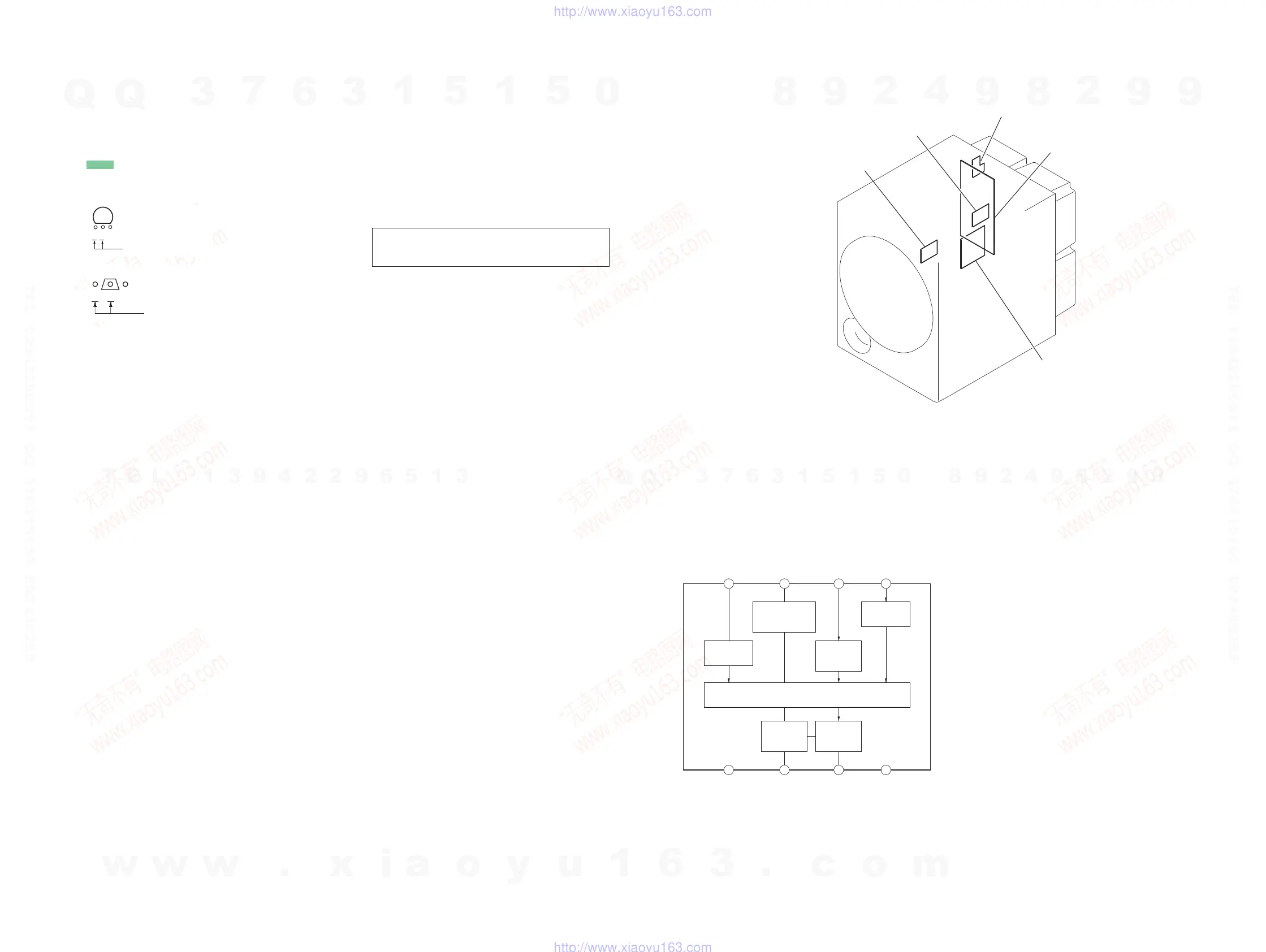
For Printed Wiring Boards.
Note:
• X : Parts extracted from the component side.
• Y : parts extracted from the conductor side.
• : Pattern from the side which enables seeing.
(The other layers' patterns are not indicated.)
• Indication of transistor.
These are omitted.
These are omitted.
Note: The components identifi ed by mark 0 or dotted
line with mark 0 are critical for safety.
Replace only with part number specifi ed.