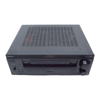
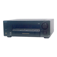
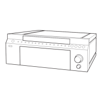
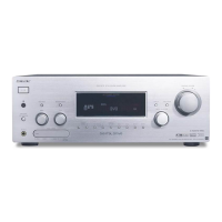
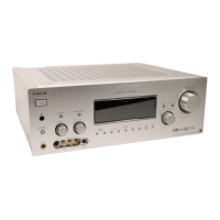
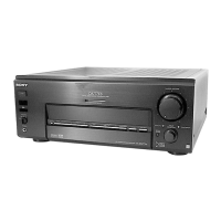
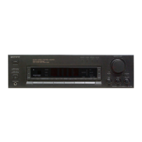
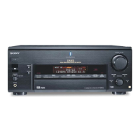
STR-DA3ES/DA5ES/VA555ES
13 13
For schematic diagrams.
Note:
• All capacitors are in µF unless otherwise noted. pF: µµF
50 WV or less are not indicated except for electrolytics
and tantalums.
• All resistors are in Ω and
1
/
4
W or less unless otherwise
specified.
• % : indicates tolerance.
• 2 : nonflammable resistor.
• 5 : fusible resistor.
• C : panel designation.
• U : B+ Line.
• V : B– Line.
• H : adjustment for repair.
• Voltages and waveforms are dc with respect to ground
under no-signal (detuned) conditions.
No mark : FM
• Voltages are taken with a VOM (Input impedance 10 MΩ).
Voltage variations may be noted due to normal produc-
tion tolerances.
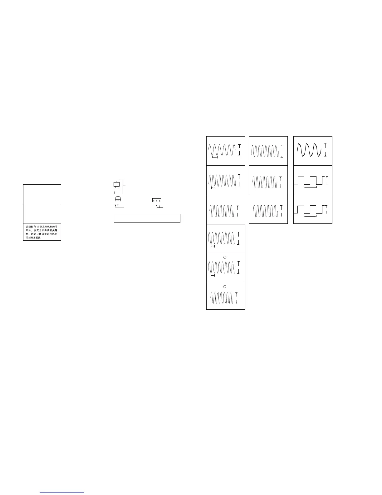
• Waveforms are taken with a oscilloscope.
• Circled numbers refer to waveforms.
• Signal path.
F : FM
J : CD (ANALOG)
c : CD (DIGITAL)
• Abbreviation
CND : Canadian model
CH : Chinese model
KR : Korea model
THIS NOTE IS COMMON FOR PRINTED WIRING
BOARDS AND SCHEMATIC DIAGRAMS.
(IN ADDITION TO THIS NECESSARY NOTE IS PRINTED
IN EACH BLOCK.)
Q
C
These are omitted
EB
E
These are omitted
CB
• Waveform
• DIGITAL SECTION
Note:
The components identified by
mark 0 or dotted line with mark
0 are critical for safety.
Replace only with part number
specified.
Note:
Les composants identifiés par
une marque 0 sont critiques
pour la sécurité.
Ne les remplacer que par une
pièce portant le numéro spécifié.
1 IC1901 qh (X OUT)
2 IC2001 tk (XO)
4 IC1201 qs (MCLK2)
5 IC1401 (MCLK2)
6 IC1501 (MCLK2)
5.0Vp-p
137nsec
7.28MHz
2.1Vp-p
14.31818MHz
3.6Vp-p
12.5MHz
1 IC209 9 (XS)
2 IC207 5
3 IC207 7
• S-VIDEO SECTION
5.0Vp-p
14.31MHz
5.0Vp-p
17.34MHz
3 IC1103 7
3.2Vp-p
24.576MHz
139
139
4.0Vp-p
20MHz
1 IC9011 4
2 IC9012 2A1
3 IC9012 3A2
• SUB DSC SECTION
3.3Vp-p
21µsec
3.3Vp-p
330nsec
There are a few cases that the part printed on
this diagram isn't mounted in the model.
For printed wiring boards.
Note:
• X : parts extracted from the component side.
• a : Through hole.
• b : Pattern from the side which enables seeing.
• There are few cases that the part isn't mounted in model is printed
on diagram.