STR-DB830/DB930/V929X
US Model
STR-DB930/DB830
Canadian Model
STR-DB930
AEP Model
STR-DB930/DB830
E Model
Australian Model
STR-DB930
Chinese Model
STR-V929X
SERVICE MANUAL
FM STEREO FM-AM RECEIVER
— Continued on next page —
SPECIFICATIONS
Manufactured under license from Dolby Laboratories
Licensing Corporation.
“DOLBY” and the double-D symbol a are trademarks
of Dolby Laboratories Licensing Corporation.
Ver 1.1 2002. 02
Sony Corporation
Home Audio Company
Published by Sony Engineering Corporation
9-928-896-12
2002B1600-1
© 2002.02
AUDIO POWER SPECIFICATIONS
POWER OUTPUT AND TOTAL HARMONIC DISTORTION : With 8
Ω
loads, both channels driven, from 20 - 20,000 Hz ; rated 110 W
(STR-DB930) and 100 W (STR-DB830) per channel minimum
RMS power, with no more than 0.05 % total harmonic distortion
from 250 mW to rated output (USA model only).
Amplifier section
POWER OUTPUT
Stereo mode
North American model
(8 Ω 20 Hz - 20 kHz, THD 0.05 %)
STR-DB930 : 110 W + 110 W
STR-DB830 : 100 W + 100 W
(4 Ω 20 Hz - 20 kHz, THD 0.05 %)
STR-DB930 : 100 W + 100 W
STR-DB830 : 90 W + 90 W
Other model
100 W + 100 W (8 ΩDIN 1kHz)
100 W + 100 W (4 ΩDIN 1kHz)
90 W + 90 W (8 Ω 20Hz-20kHz,thd0.05%)
90 W + 90 W (4 Ω 20Hz-20kHz,thd0.05%)
Surround mode
North American model
(8 Ω 20 Hz - 20 kHz, THD 0.09 %)
STR-DB930 : Front : 110 W + 110 W
Center
a)
: 110 W
Rear
a)
: 110 W + 110 W
STR-DB830 : Front : 100 W + 100 W
Center
a)
: 100 W
Rear
a)
: 100 W + 100 W
(4 Ω 20 Hz - 20 kHz, THD 0.09 %)
STR-DB930 : Front : 100 W + 100 W
Center
a)
: 100 W
Rear
a)
: 100 W + 100 W
STR-DB830 : Front : 90 W + 90 W
Center
a)
: 90 W
Rear
a)
: 90 W + 90 W
Other model
(8 Ω 20 Hz - 20 kHz, THD 0.09 %)
Front : 90 W + 90 W
Center
a)
: 90 W
Rear
a)
: 90 W + 90 W
(4 Ω 20 Hz - 20 kHz, THD 0.05 %)
Front : 90 W + 90 W
Center
a)
: 90 W
Rear
a)
: 90 W + 90 W
a) Depending on the sound field settings and the source, there may be no
sound output.
Dynamic power output
STR-DB930 : 165 W + 165 W, 8 Ω
250 W + 250 W, 4 Ω
STR-DB830 : 155 W + 155 W, 8 Ω
240 W + 240 W, 4 Ω
Frequency response
PHONO : RIAA
equalization curve ±0.5 dB
CD, TAPE, MD/DAT, TAPE/MD, DVD/LD, TV/SAT, VIDEO
1,2, andVIDEO3:
10 Hz - 50 kHz + 0.5/-2
dB(with sound field, equalizer, and
bass boost bypassed)
Inputs(Analog)
PHONO :
Sensitivity : 2.5 mV
Impedance : 50 kΩ
S/N
b)
: 86 dB(A, 2.5 mV
c)
)
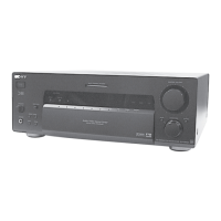
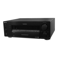
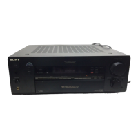
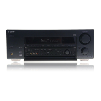
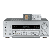
Photo : STR-DB930 (BLACK model)