Do you have a question about the Sony STR-DB825 and is the answer not in the manual?
Details power output, surround modes, and frequency response for the amplifier section.
Lists sensitivity and impedance for various audio and video inputs.
Details voltage and impedance for audio outputs and headphone compatibility.
Restores the unit to its factory default settings.
Erases all preset settings and returns the unit to its initial state.
Verifies the functionality of the fluorescent indicator tube and LEDs.
Mode for checking the functionality of all key inputs on the unit.
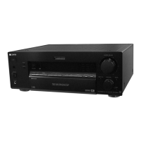
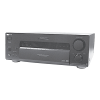
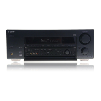
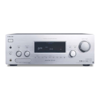
Identifies and describes the various parts and controls on the front panel.
Illustrates the physical placement of various circuit boards within the receiver.
Shows the overall signal flow and functional blocks of the main audio processing section.
Illustrates the power supply and distribution system within the receiver.
Detailed schematic of the video input signal processing circuits.
Shows the component layout for the video input circuitry.
Illustrates the component placement for the input signal processing circuits.
Detailed schematic of the S-video signal processing circuits.
Shows the component layout for the S-video signal processing circuitry.
Detailed schematic for the speaker output circuits and protection relays.
Illustrates the component placement for the speaker output circuitry.
Shows the component layout for the display control circuitry.
Detailed schematic of the display control and indicator circuits.
Schematics for various control boards on the front panel, including SW, SP SW, Balance, Vol, Function.
Component layout diagrams for front panel control boards like SW, SP SW, Balance, Vol, Function.
Detailed schematic of the main power amplifier circuits for all channels.
Component layout diagram for the main power amplifier circuitry.
Detailed schematic of the power transformer and standby circuit.
Component layout diagram for the power transformer and standby circuit.
Internal block diagrams for key integrated circuits used in the receiver.
Detailed pin functions and descriptions for the uPD780208GF IC on the Display Board.
Exploded view illustrating the assembly of the unit's case and back panel components.
Exploded view showing the components and assembly of the unit's front panel.
Exploded view illustrating the main chassis components and their arrangement.
| Number of Channels | 5.1 |
|---|---|
| Speaker load impedance | 8 ohms |
| Video Connections | Composite, S-Video |
| Power Output | 100 W per channel into 8 ohms |
| Tuning range | FM, AM |
| Frequency Response | 10 Hz - 100 kHz |
| Input Sensitivity | 200 mV |
| Output | Speaker terminals |
| Digital inputs | Optical, Coaxial |