EasyManua.ls Logo

Sony STR-DB830 Service Manual

Sony STR-DB830
64 pages
To Next Page IconTo Next Page
Page #1 background imageLoading...
Page #1 background image
STR-DB830/DB930/V929X
US Model
STR-DB930/DB830
Canadian Model
STR-DB930
AEP Model
STR-DB930/DB830
E Model
Australian Model
STR-DB930
Chinese Model
STR-V929X
SERVICE MANUAL
FM STEREO FM-AM RECEIVER
MICROFILM
— Continued on next page —
SPECIFICATIONS
Manufactured under license from Dolby Laboratories
Licensing Corporation.
“DOLBY” and the double-D symbol a are trademarks
of Dolby Laboratories Licensing Corporation.
AUDIO POWER SPECIFICATIONS
POWER OUTPUT AND TOTAL HARMONIC DISTORTION : With 8
loads, both channels driven, from 20 - 20,000 Hz ; rated 110 W
(STR-DB930) and 100 W (STR-DB830) per channel minimum
RMS power, with no more than 0.05 % total harmonic distortion
from 250 mW to rated output (USA model only).
Amplifier section
POWER OUTPUT
Stereo mode
North American model
(8 20 Hz - 20 kHz, THD 0.05 %)
STR-DB930 : 110 W + 110 W
STR-DB830 : 100 W + 100 W
(4 20 Hz - 20 kHz, THD 0.05 %)
STR-DB930 : 100 W + 100 W
STR-DB830 : 90 W + 90 W
Other model
100 W + 100 W (8 DIN 1kHz)
100 W + 100 W (4 DIN 1kHz)
90 W + 90 W (8 20Hz-20kHz,thd0.05%)
90 W + 90 W (4 20Hz-20kHz,thd0.05%)
Surround mode
North American model
(8 20 Hz - 20 kHz, THD 0.09 %)
STR-DB930 : Front : 110 W + 110 W
Center
a)
: 110 W
Rear
a)
: 110 W + 110 W
STR-DB830 : Front : 100 W + 100 W
Center
a)
: 100 W
Rear
a)
: 100 W + 100 W
(4 20 Hz - 20 kHz, THD 0.09 %)
STR-DB930 : Front : 100 W + 100 W
Center
a)
: 100 W
Rear
a)
: 100 W + 100 W
STR-DB830 : Front : 90 W + 90 W
Center
a)
: 90 W
Rear
a)
: 90 W + 90 W
Other model
(8 20 Hz - 20 kHz, THD 0.09 %)
Front : 90 W + 90 W
Center
a)
: 90 W
Rear
a)
: 90 W + 90 W
(4 20 Hz - 20 kHz, THD 0.05 %)
Front : 90 W + 90 W
Center
a)
: 90 W
Rear
a)
: 90 W + 90 W
a) Depending on the sound field settings and the source, there may be no
sound output.
Dynamic power output
STR-DB930 : 165 W + 165 W, 8
250 W + 250 W, 4
STR-DB830 : 155 W + 155 W, 8
240 W + 240 W, 4
Frequency response
PHONO : RIAA
equalization curve ±0.5 dB
CD, TAPE, MD/DAT, TAPE/MD, DVD/LD, TV/SAT, VIDEO
1,2, andVIDEO3:
10 Hz - 50 kHz + 0.5/-2
dB(with sound field, equalizer, and
bass boost bypassed)
Inputs(Analog)
PHONO :
Sensitivity : 2.5 mV
Impedance : 50 k
S/N
b)
: 86 dB(A, 2.5 mV
c)
)
Photo : STR-DB930 (BLACK model)
w
w
w
.
x
i
a
o
y
u
1
6
3
.
c
o
m
Q
Q
3
7
6
3
1
5
1
5
0
9
9
2
8
9
4
2
9
8
T
E
L
1
3
9
4
2
2
9
6
5
1
3
9
9
2
8
9
4
2
9
8
0
5
1
5
1
3
6
7
3
Q
Q
TEL 13942296513 QQ 376315150 892498299
http://www.xiaoyu163.com

Other manuals for Sony STR-DB830

Question and Answer IconNeed help?

Do you have a question about the Sony STR-DB830 and is the answer not in the manual?

Sony STR-DB830 Specifications

General IconGeneral
BrandSony
ModelSTR-DB830
CategoryStereo Receiver
LanguageEnglish

Summary

Section 1 General

Identifying the Parts Front Panel

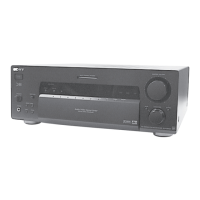
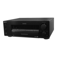
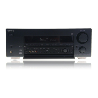
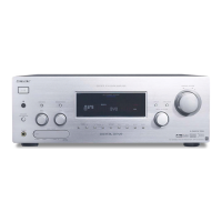
Overview of front panel components and their locations.

Section 2 Servicing Note

Servicing Notes

Important notes for servicing specific boards and ensuring proper earth connection.

Section 3 Test Mode

Fluorescent Indicator Tube Test Mode

Test to check all fluorescent display segments.

Factory Set Mode

Resets all preset contents to default settings.

All Clear Mode

Clears all preset contents, used before returning unit to client.

Sound Field Clear Mode

Clears preset sound field settings.

DSP Test Mode

Tests DSP functionality, checks data output for errors.

Autobetical Mode (AEP Model only)

Scans and sets up receivable broadcasts for Europe models.

Version Mode

Displays the microprocessor version number.

Section 4 Diagrams

4-1. Block Diagram Main Section

Overall block diagram of the main section.

4-2. Block Diagram Power Section

Block diagram of the power supply section.

4-3. Circuit Board Location

Illustrates the physical location of various circuit boards.

4-4. Schematic Diagram Digital Section (1/3)

Schematic of the digital section, part 1 of 3.

4-5. Schematic Diagram Digital Section (2/3)

Schematic of the digital section, part 2 of 3.

4-6. Schematic Diagram Digital Section (3/3)

Schematic of the digital section, part 3 of 3.

4-7. Printed Wiring Board Digital Section (1/2)

Printed wiring board layout for the digital section, part 1 of 2.

4-7. Printed Wiring Board Digital Section (2/2)

Printed wiring board layout for the digital section, part 2 of 2.

4-8. Printed Wiring Board Display Section

Printed wiring board layout for the display section.

4-10. Schematic Diagram Display Section

Schematic diagram for the display section.

4-11. Printed Wiring Board Speaker Switch Section

Printed wiring board layout for the speaker switch section.

4-12. Schematic Diagram Speaker Switch Section

Schematic diagram for the speaker switch section.

4-14. Schematic Diagram Rear Amp Section

Schematic diagram for the rear amplifier section.

4-15. Printed Wiring Board Power Section

Printed wiring board layout for the power supply section.

4-17. Printed Wiring Board Video Section

Printed wiring board layout for the video section.

4-22. IC Pin Function Description

Detailed pinout and function for integrated circuits.

4-23. IC Block Diagrams

Block diagrams illustrating the internal structure of integrated circuits.

Section 5 Exploded Views

5-1. Front Panel Section

Exploded view showing front panel components and assembly.

5-2. Chassis Section

Exploded view illustrating the internal chassis and component layout.

Related product manuals