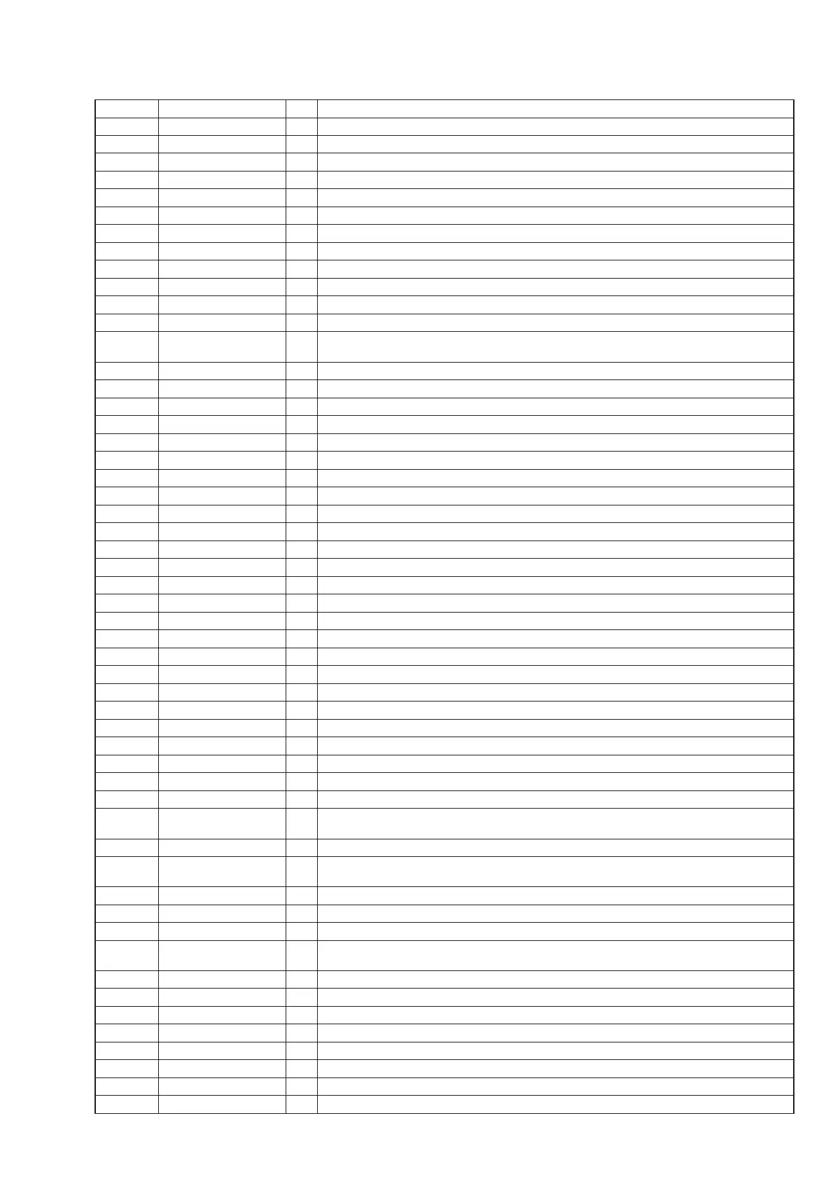
STR-DN1010
73
Pin No. Pin Name I/O Description
61 EM_D[11] I/O Two-way data bus with the SD-RAM
62 Vss - Ground terminal
63, 64 EM_D[10], EM_D[9] I/O Two-way data bus with the SD-RAM
65 CVdd - Power supply terminal (+1.2V)
66 EM_D[8] I/O Two-way data bus with the SD-RAM
67 EM_WE_DQM[1] O Byte enable signal output to the SD-RAM
68 DVdd - Power supply terminal (+3.3V)
69 Vss - Ground terminal
70 EM_CLK O Clock signal output to the SD-RAM
71 EM_CKE O Clock enable signal output to the SD-RAM
72 Vss - Ground terminal
73 DVdd - Power supply terminal (+3.3V)
74 to 76
EM_A[11], EM_A[9],
EM_A[8]
O Address signal output to the SD-RAM
77 CVdd - Power supply terminal (+1.2V)
78 Vss - Ground terminal
79, 80 EM_A[7], EM_A[6] O Address signal output to the SD-RAM
81 DVdd - Power supply terminal (+3.3V)
82 Vss - Ground terminal
83, 84 EM_A[5], EM_A[4] O Address signal output to the SD-RAM
85 CVdd - Power supply terminal (+1.2V)
86 EM_A[3] O Address signal output to the SD-RAM
87 Vss - Ground terminal
88, 89 EM_A[2], EM_A[1] O Address signal output to the SD-RAM
90 CVdd - Power supply terminal (+1.2V)
91 EM_A[0] O Address signal output to the SD-RAM
92 DVdd - Power supply terminal (+3.3V)
93 EM_A[10] O Address signal output to the SD-RAM
94 EM_BA[1] O Bank address signal output to the SD-RAM
95 Vss - Ground terminal
96 EM_BA[0] O Bank address signal output to the SD-RAM
97 EM_CS[0]# O Chip select signal output to the SD-RAM
98 EM_RAS# O Row address strobe signal output to the SD-RAM
99 Vss - Ground terminal
100 EM_CS[2]# - Not used
101 CVdd - Power supply terminal (+1.2V)
102 EM_RW - Not used
103 DVdd - Power supply terminal (+3.3V)
104 EM_OE# - Not used
105
SPI0_ENA#/
I2C1_SDA
O Chip enable signal output to the system controller
106 Vss - Ground terminal
107
SPI0_SCS#/I2C1_
SCL
I Chip select signal input from the system controller
108 SPI0_CLK/I2C0_SCL I Serial data transfer clock signal input from the system controller
109 Vss - Ground terminal
110 SPI0_SIMO I Serial data input from the system controller
111
SPI0_SOMI/
I2C0_SDA
O Serial data output to the system controller
112 DVdd - Power supply terminal (+3.3V)
113 AXR0[0] O PCM audio signal output to the stream processor
114 Vss - Ground terminal
115 AXR0[1] O PCM audio signal output to the wireless transceiver and stream processor
116 AXR0[2] O PCM audio signal output to the stream processor
117 AXR0[3] O PCM audio signal output to the wireless transceiver
118 Vss - Ground terminal
119 AXR0[4] O PCM audio signal output terminal Not used