4
TA-WR2
SECTION 2
DIAGRAMS
•Waveforms
– RX Board –
Note on Schematic Diagrams:
• All capacitors are in µF unless otherwise noted. (p: pF)
50 WV or less are not indicated except for electrolytics and
tantalums.
• All resistors are in Ω and
1
/
4
W or less unless otherwise
specified.
• f : internal component.
• 2 : nonflammable resistor.
• C : panel designation.
• A : B+ Line.
•Voltages and waveforms are dc with respect to ground
under no-signal (detuned) conditions.
no mark: Power on
•Voltages are taken with a VOM (Input impedance 10 MΩ).
Voltage variations may be noted due to normal production
tolerances.
•Waveforms are taken with a oscilloscope.
Voltage variations may be noted due to normal production
tolerances.
• Circled numbers refer to waveforms.
• Signal path.
F : AUDIO
•Abbreviation
RU : Russian model
CND : Canadian model
Note on Printed Wiring Boards:
• X : parts extracted from the component side.
• Y : parts extracted from the conductor side.
• f : internal component.
• : Pattern from the side which enables seeing.
(The other layers' patterns are not indicated.)
• Indication of transistor.
• Note for Printed Wiring Boards and Schematic Diagrams
C
B
These are omitted.
E
Q
Note:
The components identi-
fied by mark 0 or dot-
ted line with mark 0 are
critical for safety.
Replace only with part
number specified.
Note:
Les composants identifiés
par une marque 0 sont cri-
tiques pour la sécurité.
Ne les remplacer que par une
piéce portant le numéro
spécifié.
Caution:
Pattern face side: Parts on the pattern face side seen from
(SIDE A) the pattern face are indicated.
Parts face side: Parts on the parts face side seen from
(SIDE B) the parts face are indicated.
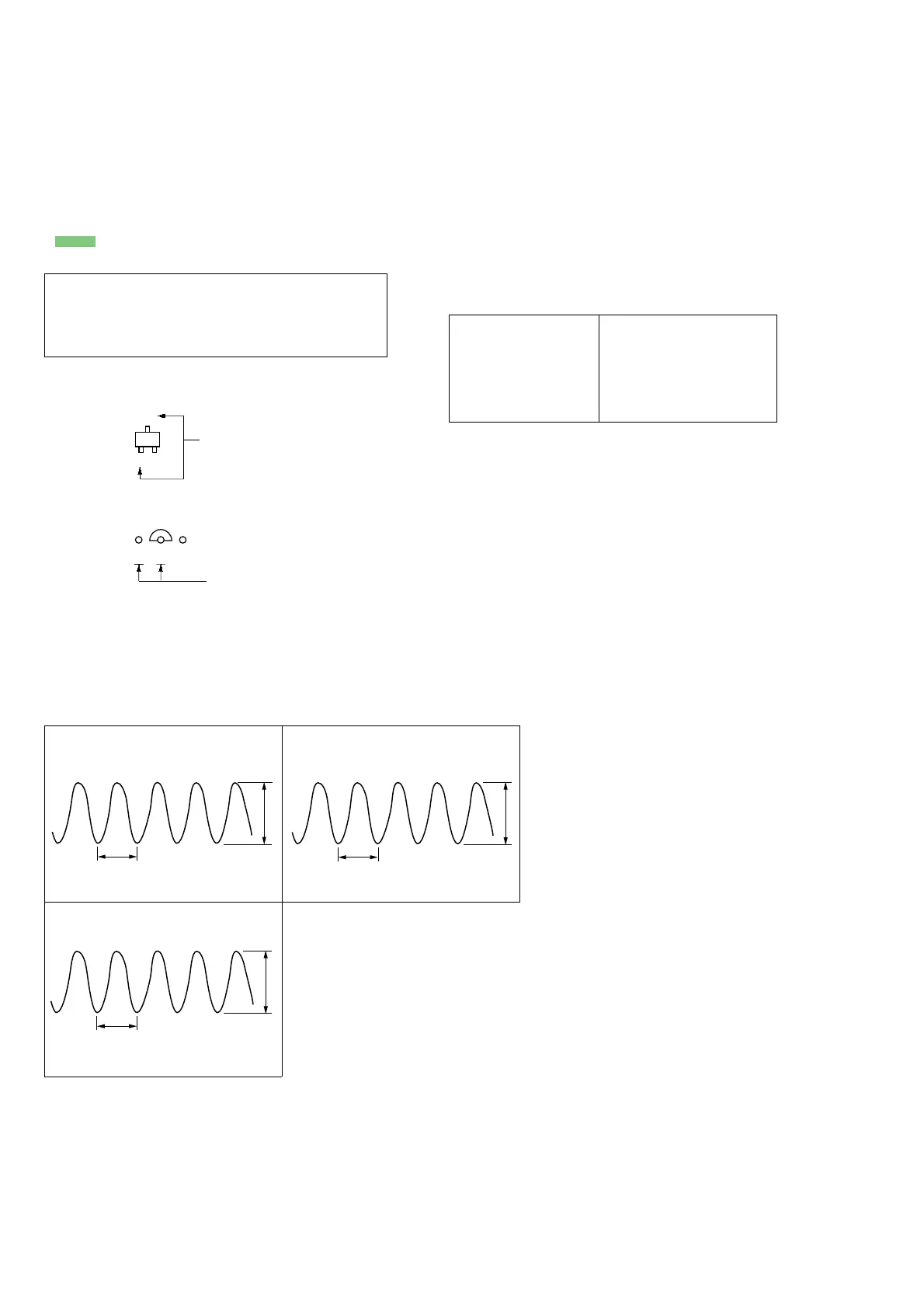
3
IC111 rk (XFSOIN)
1 V/DIV, 10 ns/DIV
2
IC102 r; (OSCI)
1
IC107 wd (X1)
1 V/DIV, 100 ns/DIV
1 V/DIV, 40 ns/DIV
125 ns
20.3 ns
81.3 ns
3.7 Vp-p
4.8 Vp-p
3.4 Vp-p
B
These are omitted.
CE
Q