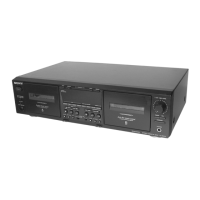
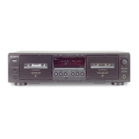
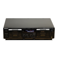
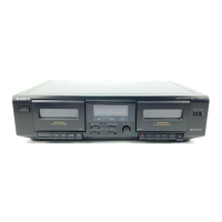
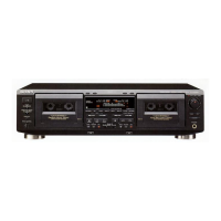
TC-WE635
WAVEFORMS
– MAIN SECTION (3/4) –
THIS NOTE IS COMMON FOR PRINTED WIRING
BOARDS AND SCHEMATIC DIAGRAMS.
(In addition to this, the necessary note is printed
in each block.)
For schematic diagrams.
Note:
• All capacitors are in µF unless otherwise noted. pF: µµF
50 WV or less are not indicated except for electrolytics
and tantalums.
• All resistors are in Ω and
1
/
4
W or less unless otherwise
specified.
• % : indicates tolerance.
•
¢
: internal component.
• 1 : fusible resistor.
• C : panel designation.
For printed wiring boards.
Note:
• X : parts extracted from the component side.
• b : Pattern from the side which enables seeing.
• Transistor of “B” and “C” indication is omitted.
• U : B+ Line.
• V : B– Line.
• H : adjustment for repair.
• Voltage is dc with respect to ground under no-signal
(detuned) condition.
no mark : STOP
( ) : REC
< > : PB
∗
: Can not be measured.
• Voltages are taken with a VOM (Input impedance 10 MΩ).
Voltage variations may be noted due to normal produc-
tion tolerances.
• Waveforms are taken with a oscilloscope.
Voltage variations may be noted due to normal produc-
tion tolerances.
• Circled numbers refer to waveforms.
• Signal path.
E : PB
a : REC
• Abbreviation
CND : Canadian model.
AUS : Australian model.
SP : Singapore model.
MY : Malaysia model.
CH : Chinese model.
• Indication of transistor
1
IC801 #ª EXTAL
Note:
The components identi-
fied by mark ! or dotted
line with mark ! are criti-
cal for safety.
Replace only with part
number specified.
Note:
Les composants identifiés par
une marque ! sont critiques
pour la sécurité.
Ne les remplacer que par une
piéce portant le numéro
spécifié.
SECTION 6
DIAGRAMS
6-1. CIRCUIT BOARDS LOCATION
4.4Vp-p
10MHz
TRANS (A) board (
4
E)
(Except SP,MY)
MAIN board
RECVOL board (
4
G)
H.P board (
4
D)
HEAD RELAY (REC/PB) board
(Deck B)
HEAD RELAY (REC/PB) board
(Deck A)
LEAF SW (REC/PB) board
(Deck B)
PANEL board (
4
A)
DIRECTION board (
4
C)
POWER board (
4
F)
LEAF SW (REC/PB) board
(Deck A)
TRANS (B) board (
4
B)
 Loading...