VPL-FX51
2-3
. Adjust GND to bottom ege
in the DC 0.5 V range.
. Probe of GND: TP5701
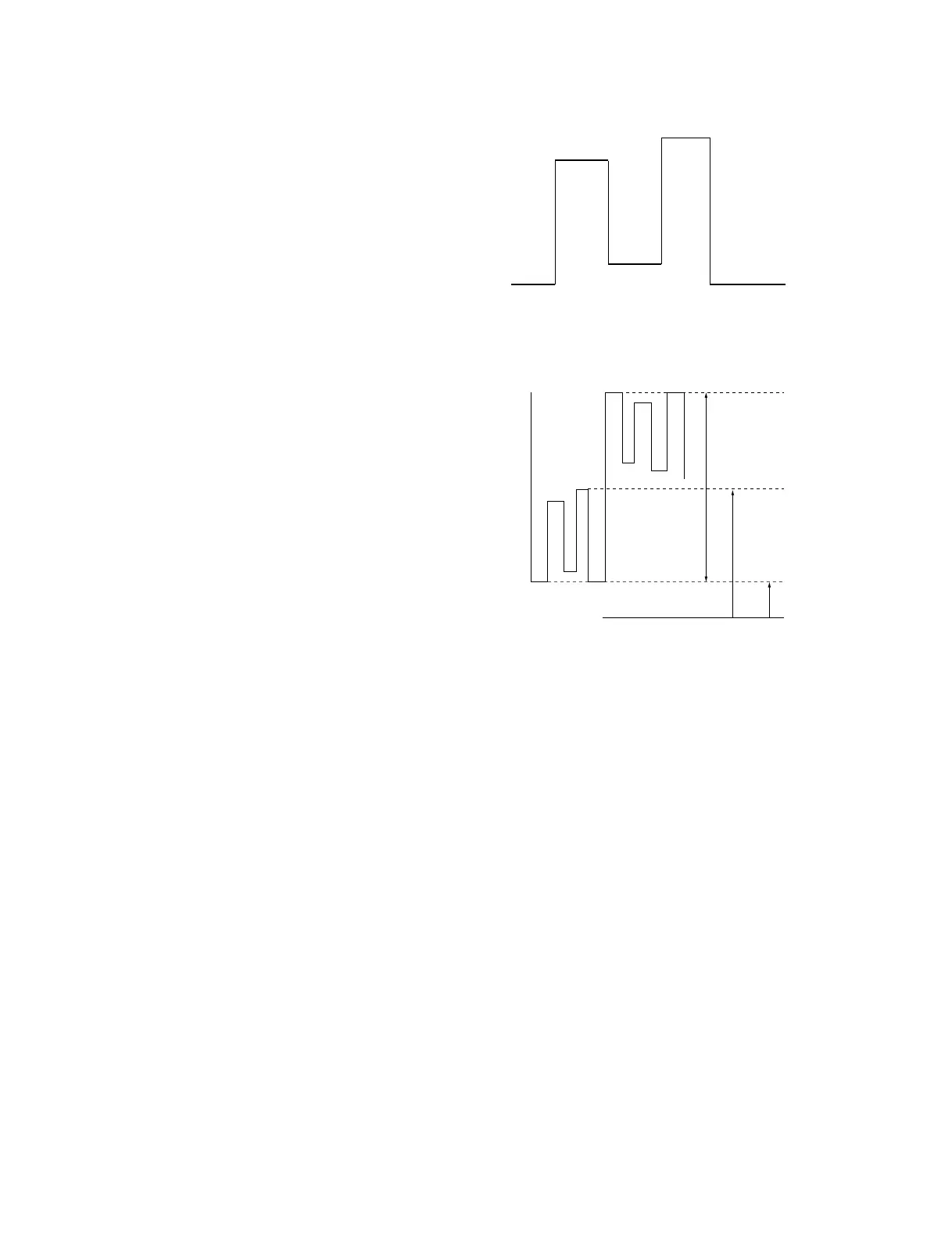
0 IRE
87.5 IRE
12.5 IRE
100 IRE
W/B HIGH adjustment signal (XGA)
7.0 ±0.05Vdc
10.0 ±0.05Vdc
0V
2.5 ±0.05Vdc
Fig. 2-5-1-1
Fig. 2-5-1-2
2-5. W/B Adjustment
2-5-1. Signal Amplitude and Center
Adjustments
1. Input the W/B HIGH adjustment signal (XGA) to
INPUT-A and connect an oscilloscope to the TP5602
on the C board.
2. Set the CONTRAST to 85.
3. Enter the item “OTHER” of Device Adjust of menu.
4. Set 07 3D GAMMA/SW: 1 to 0.
5. Set 06 3D GAMMA/THROUGH: 0 to 1.
6. Enter the item “P, DRV” of Device Adjust of menu.
7. Adjust 02.OFFSET(GE) so that the signal amplitude is
10.0 ±0.05 Vdc.
8. Adjust 27.SH/SH2G so that the 100 IRE level (lower
part of the signal) is 7.0 ±0.05 Vdc.
9. Adjust 09.SIG CEN so that the lowest of signal is 2.5
±0.05 Vdc.
10. If necessary, repeat items 7 and 8.
11. Connect an oscilloscope to the TP5702 on the C board.
12. Adjust 01.OFFSET R(E) so that the lowest of signal is
2.5 ±0.05 Vdc.
13. Adjust 26.SH/SH2R so that the 0 IRE level(the upper
part of the signal) is 12.5 ±0.05 Vdc.
14. Make sure that the 100 IRE level (lower part of the
signal) is 7.0 ±0.05 Vdc.
15. Connect an oscilloscope to the TP5802 on the C board.
16. Adjust 03.OFFSET B (E) so that the GND side is 2.5
±0.05 Vdc.
17. Adjust 28.SH/SH2B so that the 0 IRE level (upper part
of the signal) is 12.5 ±0.05 Vdc.
18. Make sure that the 100 IRE level (lower part of the
signal) is 7.0 ±0.05 Vdc.
19. Select the item “SAVE TO MEMORY” of Device
Adjust of menu. Press ENTER to save the data.
20. Return the CONTRAST to 80.
21. Reverse the top and down each 01,02 and 03 OFFSET
and duplicate them.
 Loading...