49
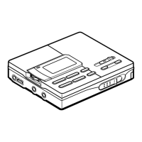
MZ-RH1
Pin No. Pin Name I/O Description
260
XPD_ADC O Power control signal output to the A/D converter
261
PAUSE_KEY I Pause key input terminal
262
XOPT_CTL O Power supply on/off control signal output terminal for the optical input jack
263
DRAM_VDD_
CLR
O Internal D-RAM power supply latch clear signal output for quick mode sleep
264
XDRAMVDD_
SEL
O Power supply control signal output terminal for the FCRAM
265
DRAM_ALONE O Power on/off control signal output terminal for internal D-RAM
266
DRAMVDD_
DISCHG
O Power supply discharge control signal output terminal for internal D-RAM
267
PCB - Not used
268
XRST_DISPLAY O Reset signal output to the display driver IC
269
PC2 - Not used
270
EX512 - Not used
271
FS256 O Master clock signal (256Fs=11.2896 MHz) output to A/D converter
272
ADDT I Data input from A/D converter
273
LRCK O L/R sampling clock signal (44.1kHz) output to external A/D converter
274
XBCK O Bit clock (2.8224 MHz) output to the external A/D converter
275
DIN I Digital audio signal input terminal
276
OSCI I Main system clock input terminal (22.5792 MHz)
277
OSCO O Main system clock output terminal (22.5792 MHz)
278
FS512 O Clock signal (512Fs=22.5792 MHz) output to the headphone amplifier
279
DCLSOUTR O PWM modulator signal output to the headphone amplifier (R-CH)
280
DCLSOUTL O PWM modulator signal output to the headphone amplifier (L-CH)
281
RMC_DTCK I/O TSB master data clock input/output or SSB data input/output with the remote commander
282
UDP I/O USB data (+) input/output terminal
283
UDM I/O USB data (-) input/output terminal
284
RREF I Connection terminal for an external resistor
285
VSENS I Connection terminal for an external resistor
286
SUSPEND O USB suspend signal output to the power control IC
287
DTL O USB pull-up resistor connection control terminal
288
USBHOLD I USB power supply separation signal input from the power control IC
289
USBOSCE I Not used
290
UOSCI I USB system clock input terminal (48 MHz) (for USB oscillation circuit)
291
UOSCO O USB system clock output terminal (48 MHz) (for USB oscillation circuit)
292
FCRAMVDD0 - Power supply terminal (FCRAM system)
293
FCRAMVSS0 - Ground terminal (for FCRAM)
294
FCRAMVDD1 - Power supply terminal (FCRAM system)
295
FCRAMVSS1 - Ground terminal (for FCRAM)
296
FLASHVDD0 - Power supply terminal (for FLASH)
297
FLASHVSS0 - Ground terminal (for FLASH)
298 to 302
PE0 to PE4 - Not used
303
MDVCC_CTL O Power supply control signal output terminal for the optical pick-up block
304
VC3_CTL O Power supply control signal output terminal Not used
305
EL_PWR_CTL O EL power supply on/off control signal output terminal
306
EBA1 - Not used
307
EBA2 - Not used
308
EBA11 - Not used
 Loading...