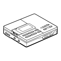
OLED BOARD IC1 S1C88317D04H000 (DISPLAY DRIVER IC)
Pin No. Pin Name I/O Description
1 to 10
COM25/SEG57 to
COM16/SEG66
- Not used
OSC3 I System clock input terminal (4 MHz)
OSC4 O System clock output terminal (4 MHz)
VD1 O Constant voltage output terminal for oscillation
VDD - Power supply terminal (+2.5V)
OSC1 I OSC1 clock signal input terminal
OSC2 O OSC1 clock signal output terminal
/TEST I Input terminal for the test Fixed at "H" in this set
/RESET I Reset signal input from the system controller
MCU//MPU I
MCU mode/MPU mode setting terminal "H": MCU mode, "L": MPU mode
Fixed at "H" in this set
XCS I Chip select signal input from the system controller
SCLK I Serial data transfer clock signal input from the system controller
SOUT O Serial data output to the system controller
SIN I Serial data input from the system controller
D7 to D0 O Serial data output to the EL display module
A0 O Address signal output to the EL display module
A1 to A18 I Address signal output terminal Not used
RD O Read strobe signal output to the EL display module
WR O Write enable signal output to the EL display module
R25 to R27, R30,
R31
- Not used
CE2, CE3 O Chip enable signal output to the EL display module
R34 to R37, R50,
R51
- Not used
COM31/SEG51 to
COM26/SEG56
- Not used
 Loading...