– 11 – – 12 – – 14 –– 13 –
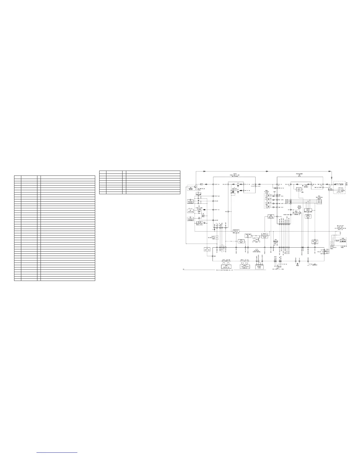
4-2. BLOCK DIAGRAM
• Signal path.
F : FM
f : AM
E : PB
• Abbreviation
CND : Canadian
EA : Saudi Arabia
CH : Chinese
9E : Indication of country of origin
5E, 6E: South America
SECTION 4
DIAGRAMS
4-1. EXPLANATION OF IC TERMINALS
IC701 TC9327AF-621 (SYSTEM CONTROL/LCD DRIVE)
Pin No. Pin Name I/O Pin Description
1– 4 COM1 – 4 O LCD driver common output.
5 – 22 S1 – 18 O LCD driver output.
23 MOTOR DIR O Motor rotation direction control output (FWD: L, REV: H).
24 MOTOR CTL O Motor ON/OFF control output (OFF: L, ON: H).
25 MOTOR SPEED O Motor speed control output (Normally: L, Speed down: H).
26 MOTOR BRK O Motor brake control output (Brake OFF: L, Brake ON: H).
27 PHOTO CTL O Photo reflector rotation detection control output.
28 DOLBY — Not used (OPEN).
29 NC — Not used (OPEN).
30 AVLS O AVLS control output (AVLS OFF: L, AVLS IN: H).
31 FM MODE O LOCAL/DX control output (DX: L, LOCAL: H) (US, CND, 5E, 6E only).
32 TAPE SELECT O Tape select control output (Normal: L, CrO2/METAL: H).
33 PHOTO IN I Photo reflector rotation detection input.
34 – 37 K0 – 3 I Key input 0 – 3.
38 NC — Not used (OPEN).
39 – 41 KO1 – 3 I Key input 1 – 3.
42 BATT DET I Power supply voltage detection input (A/D input).
43 HOLD I HOLD input.
44 RM KEY IN I Remote control key input.
45 AD REF I Reference voltage of pin 43 and 44.
46 CS O Chip select output for EEPROM.
47 DATA O Data output for EEPROM.
48 SCLK O SCLK output for EEPROM.
49 BEEP O BEEP output.
50 TEST I Test mode select terminal (Connect to remote contorol).
51 MEGA BASS O MEGA BASS control output (ON: L, OFF: H).
52 MUTE O Mute signal output (OFF: L, ON: H)
53 AMP CTL O Power AMP ON/OFF control output.
54 OPEN I OPEN switch input.
55 REV SW I Mechanism deck mode detection switch input (REV ON: H).
56 REW SW I Mechanism deck mode detection switch input (REW ON: H).
57 FF SW I Mechanism deck mode detection switch input (FF ON: H).
58 FWD SW I Mechanism deck mode detection switch input (FWD ON: H).
59 BAND O BAND select output (AM: L, FM: input).
60 RADIO ON O RADIO ON/OFF control output (OFF: L, ON: H).
61 IF REQ O IF request output (Auto scan: L, Normally: H).
62 NC — Not used (OPEN).
63 TEST/NC — Not used (OPEN).
64 IF IN I IF input.
65 PRE AMP CTL O Preamp mute signal output.
66 D02 O VT control signal output.
67 HOLD — Fixed at “H” in this set.
68 NC — Not used (OPEN).
69 GND — Ground.
70 VCO FM I VCO (FM) input.
Pin No. Pin Name I/O Pin Description
71 VCO AM I VCO (AM) input.
72 VDD — Power supply pin.
73 RESET I Reset input. Connect to VDD.
74 XOUT O Crystal oscillator output (75 kHz).
75 XIN I Crystal oscillator input (75 kHz).
76 VXT — Stabilized capacitor connection of crystal oscillation power supply.
77 VLCD — LCD driver power rising pressure pin.
78, 79 C1, 2 — LCD driver power rising pressure pin.
80 VEE — 1.5 V constant voltage power supply for LCD driver.
WM-FX491/FX491ST/FX493/FX493ST
 Loading...