– 19 – – 21 –– 20 –
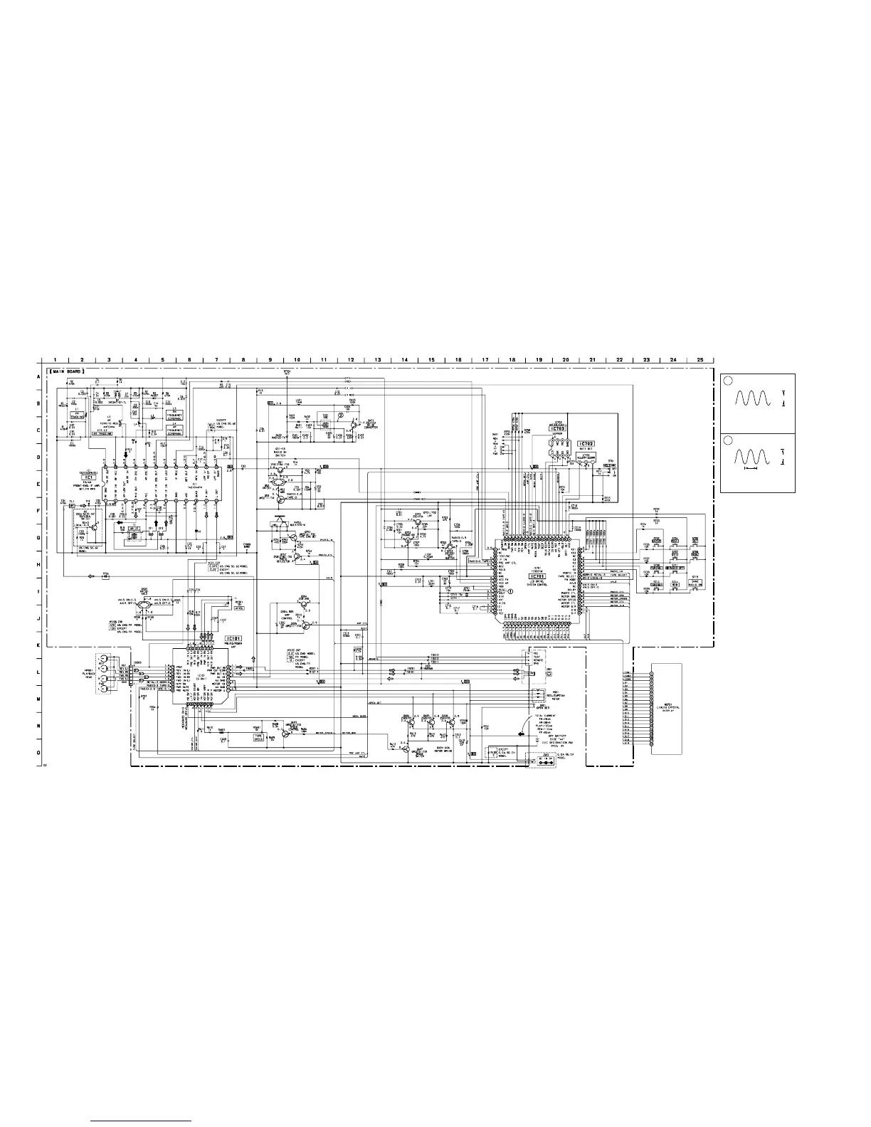
4-4. SCHEMATIC DIAGRAM
Note:
• All capacitors are in µF unless otherwise noted. pF: µµF
50 WV or less are not indicated except for electrolytics
and tantalums.
• All resistors are in Ω and
1
/
4
W or less unless otherwise
specified.
•
f
: internal component.
• U : B+ Line.
• H : adjustment for repair.
• Power voltage is dc 3V and fed with regulated dc power
supply from battery terminal.
• Voltages and waveforms are dc with respect to ground
under no-signal (detuned) conditions.
no mark : FM (RADIO SECTION)
PLAY (TAPE SECTION)
( ) : AM
• Voltages are taken with a VOM (Input impedance 10 MΩ).
Voltage variations may be noted due to normal produc-
tion tolerances.
• Waveforms are taken with a oscilloscope.
Voltage variations may be noted due to normal produc-
tion tolerances.
• Circled numbers refer to waveforms.
• Signal path.
F : FM
f : AM
E : PB
• Abbreviation
CND : Canadian
FR : French
EA : Saudi Arabia
CH : Chinese
E : Indication of country of origin
9E : No Indication of country of origin
5E, 6E: South America
CEV : Ukraine, Hungary, Czech
z
Waveforms
1
IC701 uf
XOUT
2
VOLT/DIV : 50 mV AC
TIME/DIV : 5 µsec
Q401 C
VOLT/DIV : 1 V AC
TIME/DIV : 0.1 msec
290 mVp-p
75 kHz
3.2 Vp-p
369 nsec
z
Refer to page 22 for IC Block Diagram.
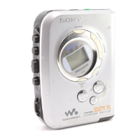
WM-FX491/FX491ST/FX493/FX493ST
 Loading...