EasyManua.ls Logo

Sony WM-D6 - Page 19

Sony WM-D6
32 pages
Print Icon
To Next Page IconTo Next Page
To Previous Page IconTo Previous Page
Loading...
WM-D6
SECTION
4
WM-D6
WM-I
DIAGRAMS
A
B
|
C
D
E
F
G
H
41,
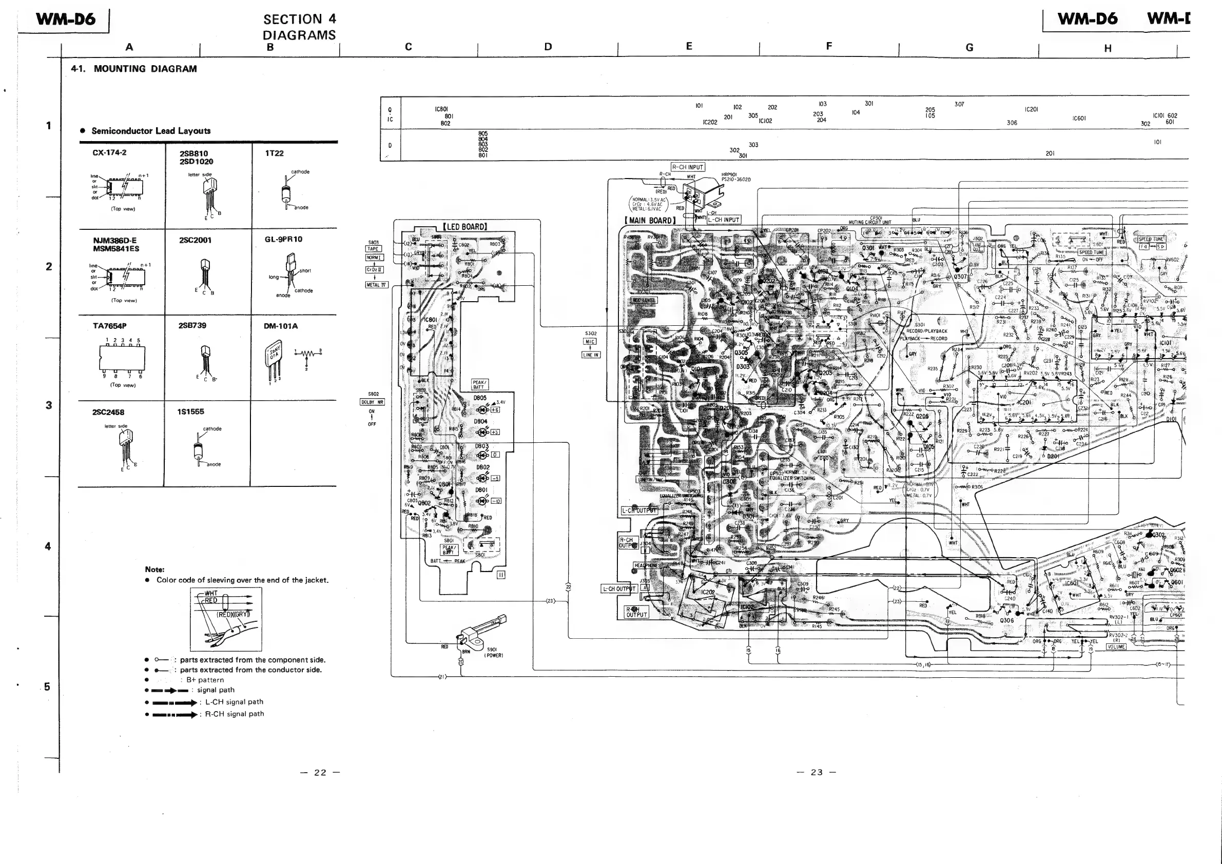
MOUNTING
DIAGRAM
Ic601
Iclor
602
1
302
~—«60!
@
Semiconductor
Lead
Layouts
101
CX-174-2
2SB810
1T22
SD
1020
-——_*
2
R-CH
INPUT
hne.
Wo
onel
letter
side
cathode
R-CH
WHT
HRP9O!
or
A
a
PS210-3602D
|
|
(RED)
SS
S
dar"
12
n
NORMAL:
3.5V.AC
gee
ii
nods
CrQ2
=
4.6V
AC
)
<>
‘op
view)
B
METAL:
6.IVAC
La
Ef
BLU
—
feel
;
ised
Gow
7164)0)
NJM386D-E
2SC2001
GL-9PR10
5803
vr
ae,
:
Gora
‘
é
gus
ea
=
aa
ee
.
se
oF
Bebe
MSM5841ES
Coe
eltenged
Ea
.
i
as
aa
SHE
Oa
OTF
coe
Vay
Lauda!
PT
eh
scorn
rwe
hos
: 5
:
:
;
ak
N=
OFF
2
line.
wnt
e
>
=
—————
vot
tp
y
is
cia
es
short
Crozet
re
——
9
shit
long
1
os
fs
METAL
IV
dot
12
n
cathode
anode
(Top
view)
TA7654P
DM-101A
12345
ee
ee
if
(ee
é
r
J
Fes
|
Rv202
5.5y
sevaea3
(Top
view)
1
Fed
ry
Ei
L
:
és
ad
é
:
Ps
~
b
9
$802
Bed,
uF
RS
few
to
eM
alte
oo
3
:
2
4
as
:
=
mo
Z
if
mcs
0)
oo
2SC2458
181555
a
it
he
2
-
*
a
[9
bE=S
aly
=
letter
side
thod
OFF
.
S
~~
ee
:
7
:
ba
av
f
A
KAS
see
&
4
©
o
=
:
cathode
R
;
*
=
5
’
4
C
i
3
2
fp
ie
9
i
a
i
:
4
>
|
we
|
A
oy
3
C220"
:
AMR.
(218
lo
a
R221
x
eo
G2N8
a
:
oS
Jan%®
,
peer
Ec
.
-
-
4
Note:
@
Color
code
of
sleeving
over
the
end
of
the
jacket.
@
O—
:
parts
extracted
from
the
component
side.
@
e—
:
parts
extracted
from
the
conductor
side.
e
:
B+
pattern
5
©
ae
>
ees:
signal
path
@
mm
meme
©
L-CH
signal
path
©
meme
smeme>
©
R-CH
signal
path