WM-EX2000
— 18 — — 19 — — 20 —
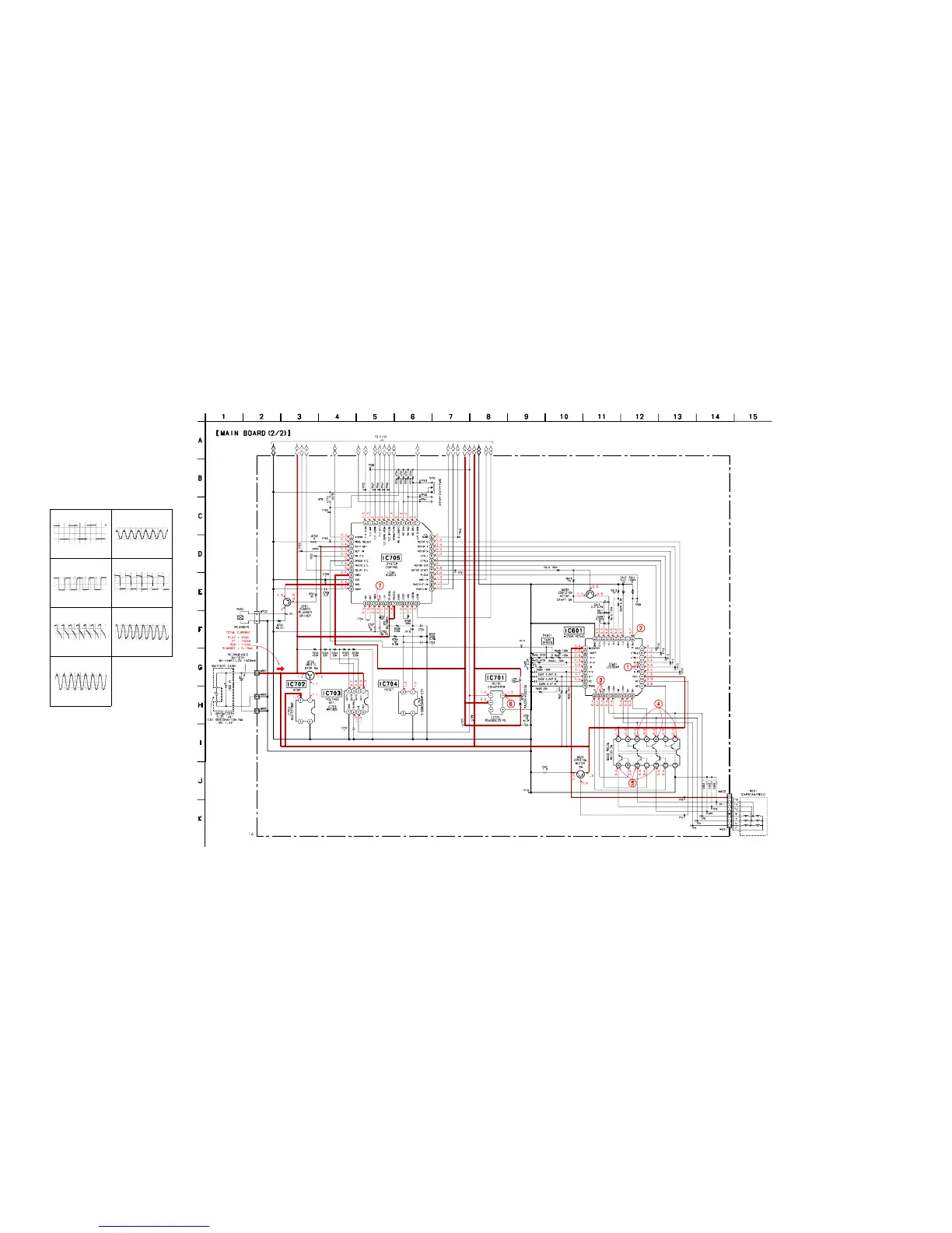
6-4. SCHEMATIC DIAGRAM MAIN (2/2) SECTION
Note on Schematic Diagram:
• All capacitors are in µF unless otherwise noted. pF: µµF
50 WV or less are not indicated except for electrolytics
and tantalums.
• All resistors are in Ω and
1
/
4
W or less unless otherwise
specified.
•
f
: internal component.
• C : panel designation.
• U : B+ Line.
• H : adjustment for repair.
• Power voltage is dc 1.3 V and fed with regulated dc power
supply from battery terminal.
• Voltages and waveforms are dc with respect to ground
under no-signal (detuned) conditions.
no mark: PLAY
• Voltages are taken with a VOM (Input impedance 10 MΩ).
Voltage variations may be noted due to normal produc-
tion tolerances.
• Waveforms are taken with a oscilloscope.
Voltage variations may be noted due to normal produc-
tion tolerances.
• Circled numbers refer to waveforms.
• Refer to page 22 for IC Block Diagrams. • Refer to page 23 for IC Pin Function Description.
• Waveform
1
IC601 456
0.5V/div
2µsec/div
2
IC601 0
0.5V/div
1µsec/div
444 Hz
150 Hz
5
Q603 80qs
0.5V/div
5µsec/div
150 Hz
3
IC601 wkwle;
0.2V/div
5µsec/div
150 Hz
150 Hz
4
Q603 135
0.5V/div
5µsec/div
6
IC701 5
1V/div
5µsec/div
100 kHz
7
IC702 wk
1V/div
0.2µsec/div
4 MHz