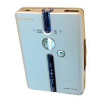
WM-EX372
– 13 –
– 14 –
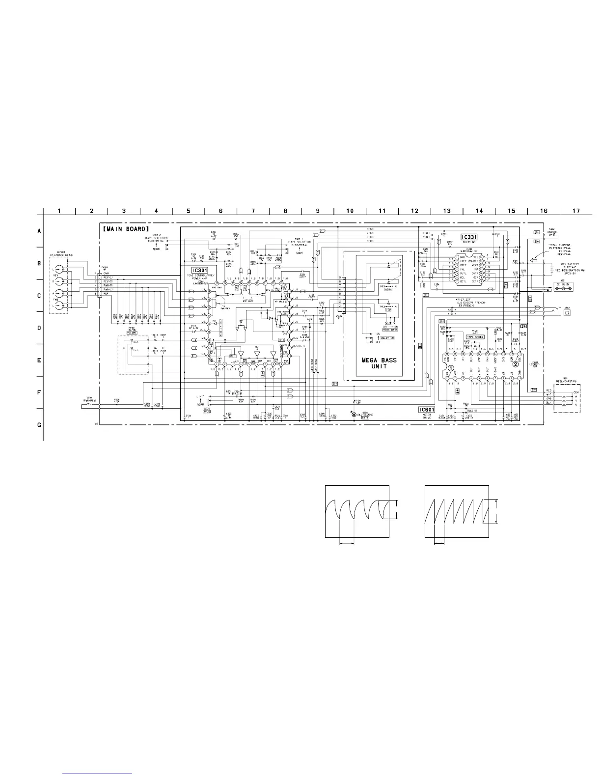
5-3. SCHEMATIC DIAGRAM • See page 15 for IC Block Diagrams.
Note on Schematic Diagram:
• All capacitors are in µF unless otherwise noted. pF: µµF
50 WV or less are not indicated except for electrolytics
and tantalums.
• All resistors are in Ω and
1
/
4
W or less unless otherwise
specified.
• C : panel designation.
• U : B+ Line.
• H : adjustment for repair.
• Total current is measured with no cassette installed.
• Power voltage is dc 3 V and fed with regulated dc power
supply from external power voltage jack.
• Voltages and waveforms are dc with respect to ground in
playback mode.
no mark : PB (FWD)
( ) : PB (REV)
• Voltages are taken with a VOM (Input impedance 10 MΩ).
Voltage variations may be noted due to normal produc-
tion tolerances.
• Waveforms are taken with a oscilloscope.
Voltage variations may be noted due to normal produc-
tion tolerances.
• Circled numbers refer to waveforms.
• Signal path.
E : PB
• Waveforms
1 IC601 1 (WB)
100 mV/DIV, 2 ms/DIV
2 IC601 !¡ (OSC)
10 mV/DIV, 1 ms/DIV

 Loading...