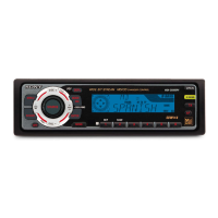
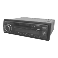
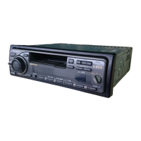
XR-C5300X/C5305/C5600X
20 20
THIS NOTE IS COMMON FOR PRINTED WIRING
BOARDS AND SCHEMATIC DIAGRAMS.
(In addition to this, the necessary note is printed
in each block.)
For schematic diagrams.
Note:
• All capacitors are in µF unless otherwise noted. pF: µµF
50 WV or less are not indicated except for electrolytics
and tantalums.
• All resistors are in Ω and
1
/
4
W or less unless otherwise
specified.
• C : panel designation.
• U : B+ Line.
• Power voltage is dc 14.4V and fed with regulated dc power
supply from ACC and BATT cords.
• Voltages and waveforms are dc with respect to ground
under no-signal (detuned) conditions.
no mark: FM
( ) : AM (MW/SW)
< > : TAPE PLAYBACK
∗
: Impossible to measure
• Voltages are taken with a VOM (Input impedance 10 MΩ).
Voltage variations may be noted due to normal produc-
tion tolerances.
• Waveforms are taken with a oscilloscope.
Voltage variations may be noted due to normal produc-
tion tolerances.
• Circled numbers refer to waveforms.
• Signal path.
F : FM
f : AM (MW/SW)
E : TAPE PLAYBACK
For printed wiring boards.
Note:
• X : parts extracted from the component side.
• Y : parts extracted from the conductor side.
• b : Pattern from the side which enables seeing.
(The other layers' patterns are not indicated.)
Caution:
Pattern face side: Parts on the pattern face side seen from the
(Conductor Side) pattern face are indicated.
Parts face side: Parts on the parts face side seen from the
(Component Side ) parts face are indicated.
1
2
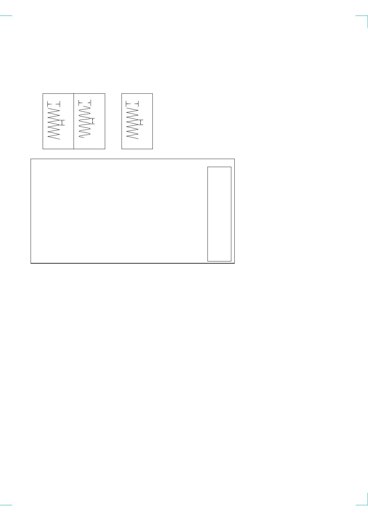
WAVEFORMS
– MAIN BOARD –
IC501 qd (OSC IN)
IC501 qg (X IN)
30.5 µsec
2.2Vp-p
1
– KEY BOARD –
IC901 y; (OSC)
0.58 µsec
1.1Vp-p
27 µsec
2.7Vp-p
 Loading...