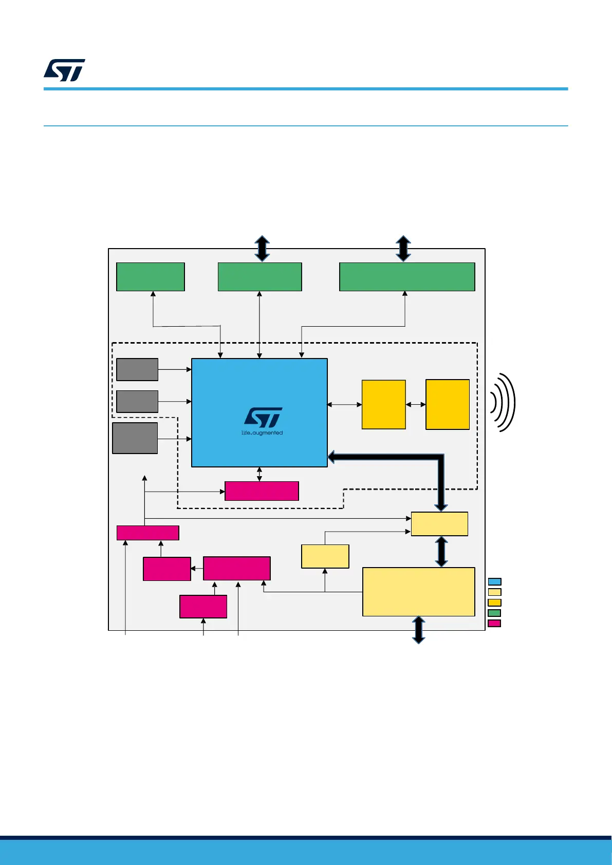
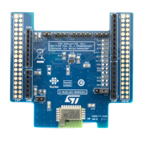
7 Hardware layout and configuration
NUCLEO-WBA55CG is designed around the STM32WBA55CG. The design includes a mezzanine board and an
MCU RF board. The hardware block diagram in Figure 2 illustrates the connection between STM32WBA55CG
and peripherals (ARDUINO
®
Uno V3 connectors, ST morpho connector, and embedded ST-LINK).
Figure 3 and Figure 5 help users locate these features on the NUCLEO-WBA55CG board. The mechanical
dimensions of the STM32WBA55CG product are shown in Figure 6.
Figure 2. Hardware block diagram
DT59347V1
PCB
antenna
STLINK-V3EC
Level shifter
Three
LEDs
Three push-buttons
ARDUINO
®
expansion connectors
32 MHz
crystal
ST morpho
expansion connectors
STM32WBA55
Filter
matching
32.768 kHz
crystal
LDO
12 to 5 V
Reset
push-button
STM32WBA55
Debug
RF path
GPIOs
Power management
VDD and V_TARGET
5V ST-LINK
ST-LINK USB
NUCLEO-WBA55CG (MB1801+MB1803)
MB1803
LDO
5 to 3 V
LDO
5 to 3 V
External
power
supply
(1.8 to 3.3 V
optional)
Power selector
ST-LINK side
STM32WBA55 side
External components
for SMPS
MB1801
Level shifter
Power selector
External
power
supply
(7 to 12 V
optional)
External
power
supply
(5 V
optional)
UM3301
Hardware layout and configuration
UM3301 - Rev 1
page 8/45