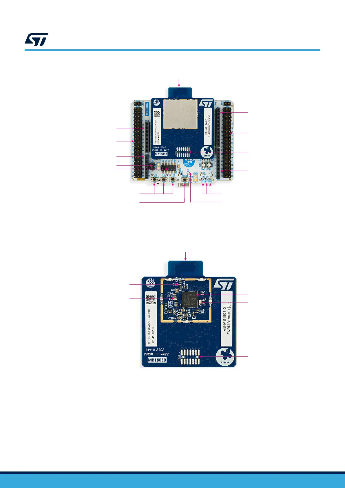
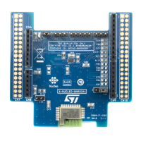
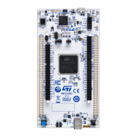
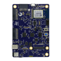
Figure 3. NUCLEO-WBA55CG PCB top view
DT59348V1
User push-buttons (B1, B2, and B3) User LEDs (LD1, LD2, and LD3)
Reset push-button (B4)
ST-LINK status LED (LD4)
VDD jumper (JP2)
5V source selector (JP1)
ST morpho (CN3)
ARDUINO
®
Power (CN5)
ST morpho (CN4)
PCB antenna
MIPI10/STDC14
connector footprint
ARDUINO
®
Analog (CN7)
ARDUINO
®
Digital 8-15 (CN6)
ARDUINO
®
Digital 0-7 (CN8)
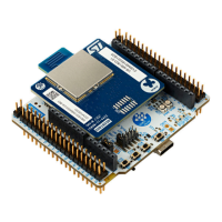
Figure 4. NUCLEO-WBA55CG PCB details of the MCU RF board
DT59349V1
PCB antenna
MIPI10/STDC14
connector footprint
STM32WBA55CG (U1)
LSE crystal (32.768 kHz)
HSE crystal (32 MHz)
C12/L1/C13/L2/C14
Matching network and filter
UM3301
Hardware layout and configuration
UM3301 - Rev 1
page 9/45


 To Next Page