Register descriptions PM0075
24/31 Doc ID 17863 Rev 1
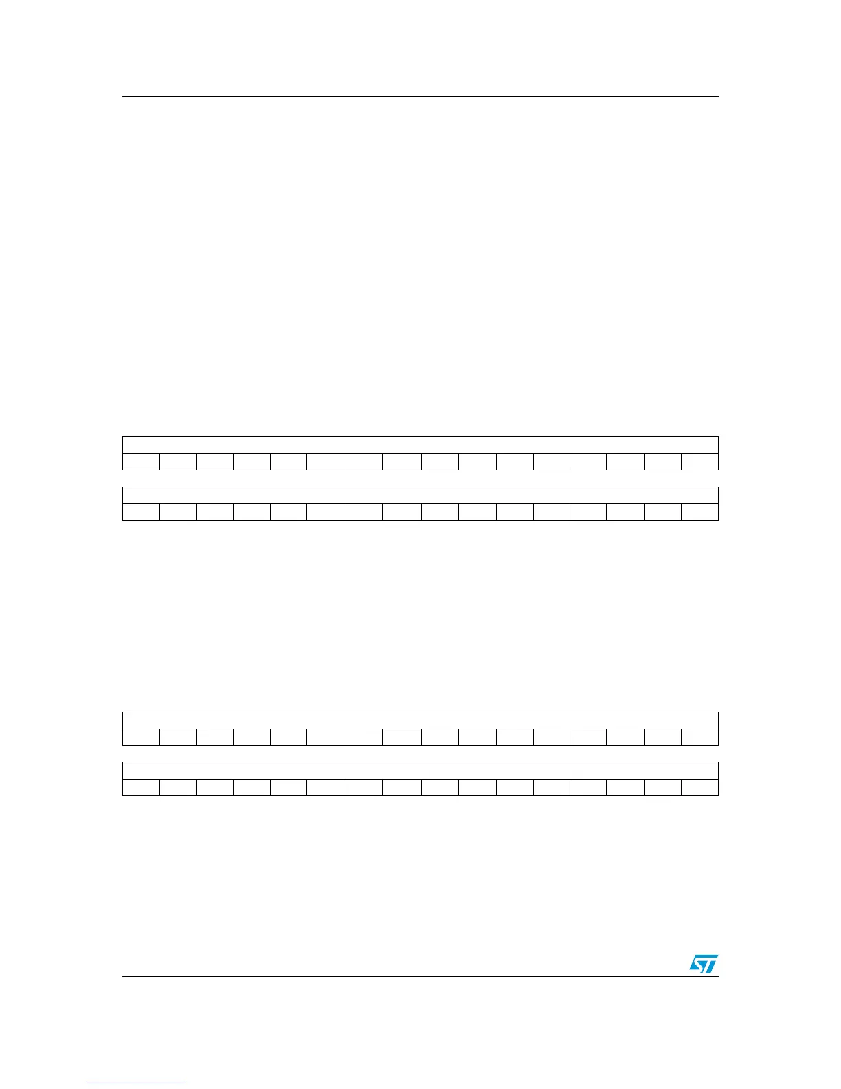
3.2 FPEC key register (FLASH_KEYR)
Address offset: 0x04
Reset value: xxxx xxxx
Note: These bits are all write-only and will return a 0 when read.
3.3 Flash OPTKEY register (FLASH_OPTKEYR)
Address offset: 0x08
Reset value: xxxx xxxx
Note: These bits are all write-only and will return a 0 when read.
Bit 4 PRFTBE: Prefetch buffer enable
0: Prefetch is disabled
1: Prefetch is enabled
Bit 3 HLFCYA: Flash half cycle access enable
0: Half cycle is disabled
1: Half cycle is enabled
Bits 2:0 LATENCY: Latency
These bits represent the ratio of the SYSCLK (system clock) period to the Flash access
time.
000 Zero wait state, if 0 < SYSCLK≤ 24 MHz
001 One wait state, if 24 MHz < SYSCLK ≤ 48 MHz
010 Two wait states, if 48 MHz < SYSCLK ≤ 72 MHz
31 30 29 28 27 26 25 24 23 22 21 20 19 18 17 16
FKEYR[31:16]
wwwwwww w wwwwwwww
15 14 13 12 11 10 9 8 7 6 5 4 3 2 1 0
FKEYR[15:0]
wwwwwww w wwwwwwww
Bits 31:0 FKEYR: FPEC key
These bits represent the keys to unlock the FPEC.
31 30 29 28 27 26 25 24 23 22 21 20 19 18 17 16
OPTKEYR[31:16]
wwwwwww w wwwwwwww
15 14 13 12 11 10 9 8 7 6 5 4 3 2 1 0
OPTKEYR[15:0]
wwwwwww w wwwwwwww
Bits 31:0 OPTKEYR: Option byte key
These bits represent the keys to unlock the OPTWRE.
 Loading...