Register descriptions PM0075
26/31 Doc ID 17863 Rev 1
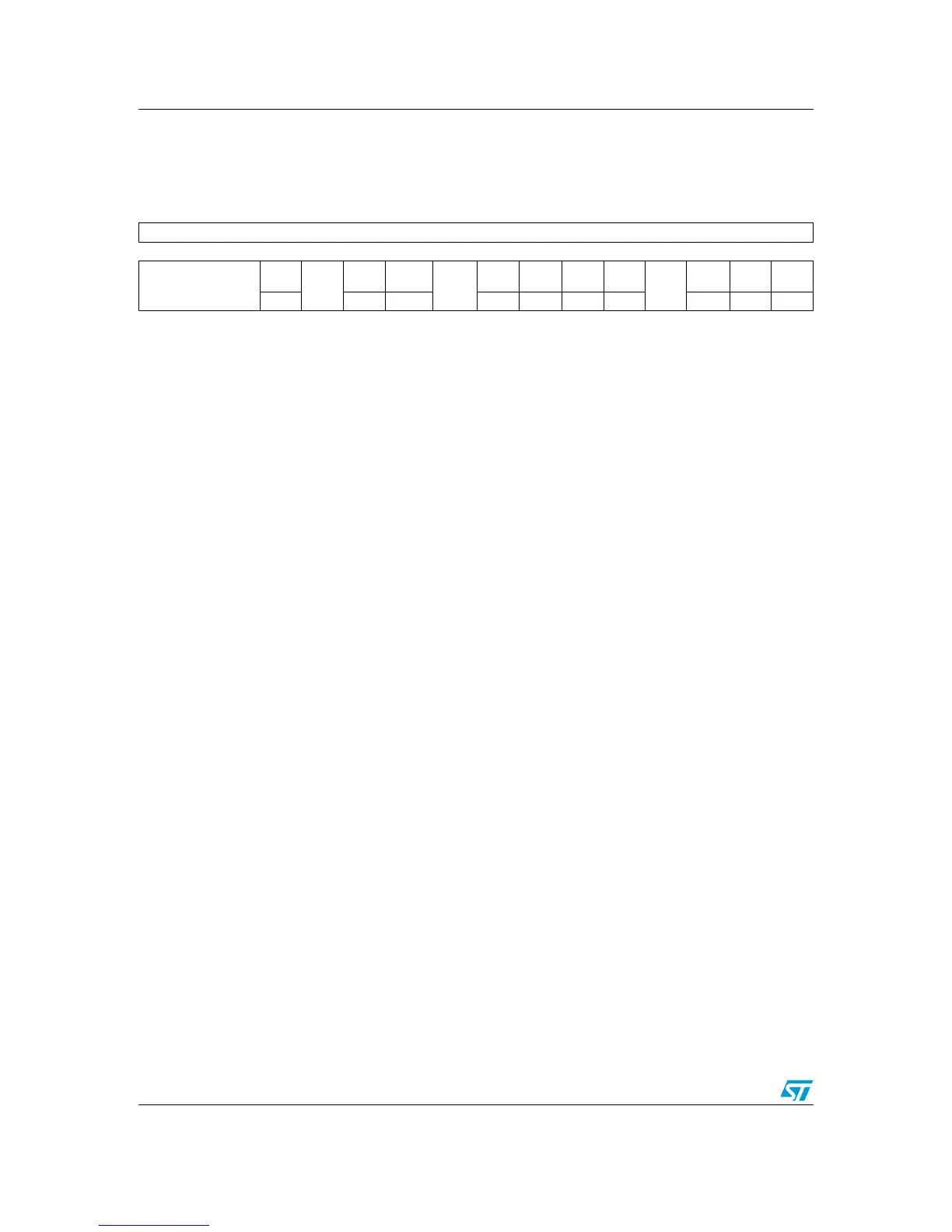
3.5 Flash control register (FLASH_CR)
Address offset: 0x10
Reset value: 0x0000 0080
31 30 29 28 27 26 25 24 23 22 21 20 19 18 17 16
Reserved
15 14 13 12 11 10 9 8 7 6 5 4 3 2 1 0
Reserved
EOPIE
Res.
ERRIE
OPTWR
E
Res.
LOCK STRT OPTER
OPT
PG
Res.
MER PER PG
rw rw rw rw rw rw rw rw rw rw
Bits 31:13 Reserved, must be kept cleared.
Bit 12 EOPIE: End of operation interrupt enable
This bit enables the interrupt generation when the EOP bit in the FLASH_SR register goes
to 1.
0: Interrupt generation disabled
1: Interrupt generation enabled
Bit 11 Reserved, must be kept cleared
Bit 10 ERRIE: Error interrupt enable
This bit enables the interrupt generation on an FPEC error (when PGERR / WRPRTERR are
set in the FLASH_SR register).
0: Interrupt generation disabled
1: Interrupt generation enabled
Bit 9 OPTWRE: Option bytes write enable
When set, the option bytes can be programmed. This bit is set on writing the correct key
sequence to the FLASH_OPTKEYR register.
This bit can be reset by software
Bit 8 Reserved, must be kept cleared.
Bit 7 LOCK: Lock
Write to 1 only. When it is set, it indicates that the FPEC and FLASH_CR are locked. This bit
is reset by hardware after detecting the unlock sequence.
In the event of unsuccessful unlock operation, this bit remains set until the next reset.
Bit 6 STRT: Start
This bit triggers an ERASE operation when set. This bit is set only by software and reset
when the BSY bit is reset.
Bit 5 OPTER: Option byte erase
Option byte erase chosen.
Bit 4 OPTPG: Option byte programming
Option byte programming chosen.
Bit 3 Reserved, must be kept cleared.
Bit 2 MER: Mass erase
Erase of all user pages chosen.
Bit 1 PER: Page erase
Page Erase chosen.
Bit 0 PG: Programming
Flash programming chosen.

 Loading...