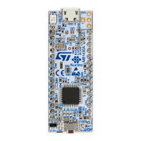
The ST STM32F407 Evaluation Board is a development system designed for the STM32F407 microcontroller. This board features an STM32F407 CPU in an LQFP176 package, along with a 20-pin Cortex Debug + ETM Connector. It allows for the development and testing of applications that can run from either the internal CPU flash or the internal SRAM.
Package Content:
The evaluation board package includes:
- STM32F4 Target board
- Power supply
- User manual
The ordering code for this package is ITSTM32F407.
Important Technical Specifications:
- Supply Voltage: 6-12V DC, @ 500 mA, with a positive center pin.
- Board Size: 106 mm x 86 mm.
- Microcontroller: STM32F407IGT6 (LQFP176 package).
- Debug Connections: 20-pin Cortex Debug + ETM Connector.
Usage Features:
Power Supply:
The permissible input voltage for the board is 6-12V DC, with the positive terminal in the center. The required current load capacity of the power supply depends on the specific configuration of the target board. A power supply with a minimum capacity of 500mA is recommended and is included in the package.
Power-Up Procedure:
- First, connect the AC power supply to the mains and then to the target board.
- Switch on the target board.
- A lit power indicator (LD2) signifies the presence of 3.3V.
Connecting an External Debugger:
When connecting an external debugger:
- Switch on the debugger before powering on the target board.
- When powering down the system, power off the target board before powering off the debugger.
Status Indicators:
- LD2 LED: Indicates the presence of the 3.3V supply voltage.
- LD1 LED: Connected to PB9.
Connectors:
20-pin Cortex Debug + ETM Connector:
This connector provides various signals for debugging and tracing. The pinout is as follows:
- Pin 1: VCC
- Pin 2: SWDIO / TMS
- Pin 3: GND
- Pin 4: SWDCLK / TCK
- Pin 5: GND
- Pin 6: SWO / TDO / EXTa / TRACECTL
- Pin 7: KEY
- Pin 8: NC / EXTb / TDI
- Pin 9: GNDDetect
- Pin 10: nRESET
- Pin 11: GND / TgtPwr + Cap
- Pin 12: TRACECLK
- Pin 13: GND / TgtPwr + Cap
- Pin 14: TRACEDATA[0]
- Pin 15: GND
- Pin 16: TRACEDATA[1]
- Pin 17: GND
- Pin 18: TRACEDATA[2]
- Pin 19: GND
- Pin 20: TRACEDATA[3]
USB Connector:
This connector is placed on the target board solely for CPU communication purposes. It cannot be used to power the target board. The pin assignments are:
- CPU Pin 122 (PA11): USB_DM
- CPU Pin 123 (PA12): USB_DP
- CPU Pin 120 (PA9): USBPWR
ETH Connector:
This connector is not populated on the board.
- SW2: Functions as a RESET button.
Jumpers:
- J2: Controls boot mode 0.
- J3: Controls boot mode 1.
For utilizing different boot modes, refer to the microcontroller reference manual.
CPU Expansion Connection:
The target board exposes most of the STM32F407 pins/signals, facilitating easy expansion of the development system. These are categorized into U4 - ANALOG, U5 - COMMUNICATION, and U6 - DIGITAL.
U4 - ANALOG Connector Pinout:
This connector provides access to various analog-related pins.
- Pin 1-2: PF3, GND
- Pin 3-4: PF4, GND
- Pin 5-6: PF5, GND
- Pin 7-8: PF6, GND
- Pin 9-10: PF7, GND
- Pin 11-12: PF8, GND
- Pin 13-14: PF9, GND
- Pin 15-16: PF10, GND
- Pin 17-18: PC0, GND
- Pin 19-20: PA3, GND
- Pin 21-22: PA4, GND
- Pin 23-24: PA5, GND
- Pin 25-26: PA6, GND
- Pin 27-28: PB0, GND
- Pin 29-30: PB1, GND
- Pin 31-32: GND, GND
- Pin 33-34: FREE, FREE
- Pin 35-36: FREE, FREE
- Pin 37-38: FREE, FREE
- Pin 39-40: FREE, FREE
U5 - COMMUNICATION Connector Pinout:
This connector provides access to various communication-related pins.
- Pin 1-2: 3V3, 3V3
- Pin 3-4: GND, GND
- Pin 5-6: PC7, PC6 (CPU Pin 116, 115)
- Pin 7-8: PC9, PC8 (CPU Pin 118, 117)
- Pin 9-10: GND, PI1 (CPU Pin 132)
- Pin 11-12: PI3, PI2 (CPU Pin 134, 133)
- Pin 13-14: GND, PC10 (CPU Pin 139)
- Pin 15-16: PC11, PC12 (CPU Pin 140, 141)
- Pin 17-18: GND, PD0 (CPU Pin 142)
- Pin 19-20: PD1, PD3 (CPU Pin 143, 145)
- Pin 21-22: PD4, GND (CPU Pin 146)
- Pin 23-24: PD5, PD6 (CPU Pin 147, 150)
- Pin 25-26: PD7, PB5 (CPU Pin 151, 164)
- Pin 27-28: PB6, PB7 (CPU Pin 164, 165)
- Pin 29-30: GND, GND
- Pin 31-32: FREE, FREE
- Pin 33-34: FREE, FREE
- Pin 35-36: FREE, FREE
- Pin 37-38: FREE, FREE
- Pin 39-40: FREE, FREE
U6 - DIGITAL Connector Pinout:
This connector provides access to various digital pins.
- Pin 1-2: 5V, 5V
- Pin 3-4: 19V, GND
- Pin 5-6: PG8, PG7 (CPU Pin 112, 111)
- Pin 7-8: PG6, PG5 (CPU Pin 110, 109)
- Pin 9-10: PG4, PG3 (CPU Pin 108, 107)
- Pin 11-12: PG2, PD15 (CPU Pin 106, 105)
- Pin 13-14: PD14, PD13 (CPU Pin 104, 101)
- Pin 15-16: PD12, PD11 (CPU Pin 100, 99)
- Pin 17-18: PD10, PD9 (CPU Pin 98, 97)
- Pin 19-20: PD8, PB13 (CPU Pin 96, 93)
- Pin 21-22: PB12, PH12 (CPU Pin 92, 89)
- Pin 23-24: PH11, PH10 (CPU Pin 88, 87)
- Pin 25-26: PH9, PH8 (CPU Pin 86, 85)
- Pin 27-28: PB11, PB10 (CPU Pin 80, 79)
- Pin 29-30: PE15, PE14 (CPU Pin 78, 77)
- Pin 31-32: PE13, PE12 (CPU Pin 75)
- Pin 33-34: PE11, PE10 (CPU Pin 73)
- Pin 35-36: PE9, PE8 (CPU Pin 69)
- Pin 37-38: FREE, 3V3
- Pin 39-40: GND, GND
Maintenance Features:
The document does not explicitly detail maintenance features beyond proper power-up and power-down procedures when using an external debugger, which helps prevent damage to the system. The design allows for easy expansion, suggesting a modular approach to development and potential troubleshooting.