27
Chapter 2: Installation
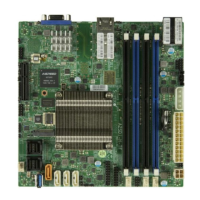
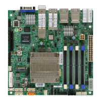
JDC
JCOM1
J3
JF1
J6
1
Rev:1.00
DESIGNED IN USA
A2SAP-L
BT1
JLCDPWR1
SRW2
SRW1
JPWR1
JLAN2
JLAN1
JEIO1
JUSB1
JHDMI1
LVDS1
I-SATA1
JGP1
JMP1
JMD1
1
2
1. JUSB1
2. JDC
Back Panel USB 3.0
Pin Denition
Pin# Denition Pin# Denition
A1 VBUS B1 VBUS
A2 D1-N B2 D2-N
A3 D1-P B3 D2-P
A4 GND B4 GND
A5 Stda_SSRX1-N B5 Stda_SSRX2-N
A6 Stda_SSRX1-P B6 Stda_SSRX2-P
A7 GND_DRAIN B7 GND_DRAIN
A8 Stda_SSTX1-N B8 Stda_SSTX2-N
A9 Stda_SSTX1-P B9 Stda_SSTX2-P
Universal Serial Bus (USB) Ports
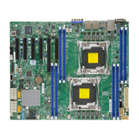
There are two USB 3.0 ports (JUSB1) on the I/O back panel. The motherboard has two
additional USB 2.0 connections via the JEIO1 header. J6 also provides two front panel USB
2.0 connections. The onboard headers can be used to provide front side USB access with a
cable. Two USB 2.0 cables for front panel support are included with the motherboard.
JDC
This is a DC jack that functions as the 12V power connector.
12V Stdby Power
Pin Denition
Pin# Denition
1 P12VSB
2 GND
3 GND
Front Panel USB 2.0 Header
Pin Denition
Pin# Denition Pin# Denition
1 P5V_DUAL_F 2 P5V_DUAL_F
3 USBCON_N4 4 USBCON_N5
5 USBCON_P4 6 USBCON_P5
7 Ground 8 Ground
9 NC 10 NC
 Loading...