XT-3 Reader Installation Manual & Data Sheet Doc no. 11-267 02
© TagMaster NA 16 (28)
5.2.3.1 Wiegand Interface
Table 4 Wiegand, Group J2
Pin Signal Description
1 D0 Wiegand 0 (zero) signal
2 D1 Wiegand 1 signal
3 CL Card load signal
4 GND Ground
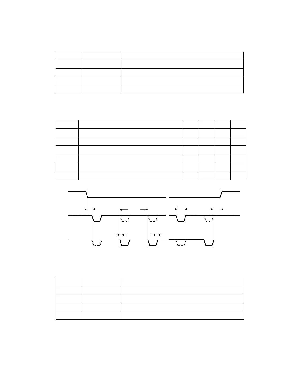
5.2.3.2 Wiegand Timing
The following values apply when all outputs are pulled up to 5V with 1kΩ resistors.
Table 5 Wiegand interface timing
Symbol
Parameter Min Typ Max Unit
t
SU
CL to D# setup time 0
µs
t
F
Fall time (all signals) 125 ns
t
R
Rise time (all signals) 5
µs
t
PI
Pulse interval 2 ms
t
PW
Pulse width 80
µs
t
H
CL hold time after last D# change 0
µs
t
SU
t
PI
t
PW
t
H
t
R
t
F
CL
D0
D1
≈
≈
≈
Figure 6 Wiegand timing diagram
5.2.3.3 Mag-stripe Interface
Table 6 Mag-stripe, Group J2
Pin Signal Description
1 CLK Mag-stripe clock signal
2 DATA Mag-stripe data signal
3 LOAD Card load signal
4 GND Ground