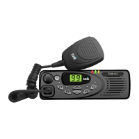
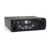
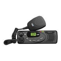
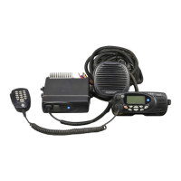
TM8100 Mobile Radio Service Manual Circuit Descriptions 67
May 2004 © Tait Electronics Limited
Automatic Gain Control The receiver has an AGC circuit to enable it to cover a large signal range.
Most of the circuit functions are implemented in the FPGA. The FPGA
passes the AGC signal to the CODEC IC204 for output from pin 14
(
IDACOUT) and thence via IC201 as the signal CDC RX AGC to pin 23 of the
quadrature mixer IC400. As the antenna signal increases, the AGC
voltage decreases.
Channel Filtering The channel filtering is split between the first and third IF stages. The
channel filtering circuit in the first IF stage comprises a pair of two-pole
crystal filters. The first filter has a 3 dB bandwidth of 12 kHz, and the
second a 3 dB bandwidth of 15 kHz. Most of the channel filtering,
however, is implemented in the FPGA. When the radio is programmed,
the different filters are selected as assigned by the channel programming.
The selectable filters plus the fixed crystal filters result in the following
total IF 3 dB bandwidths:
■ wide channel spacing : 12.6 kHz
■ medium channel spacing: 12.0 kHz
■ narrow channel spacing : 7.8 kHz
(The FPGA runs from the
DIG SYS CLK signal, which has a frequency of
12.288 MHz.) The receiver requires the TCXO calibration to be
completed to ensure that the channel filtering is centred, thereby
minimising distortion.
Received Signal
Strength Indication
The RSSI is calculated in the FPGA and DSP, and can be passed as an
analogue voltage to the internal options interface and the external
auxiliary interface. To obtain an accurate estimate of the RSSI (over the
signal level and frequency), it is necessary to calibrate the AGC
characteristic of the receiver and the front-end gain versus the receive
frequency.
3.4 Frequency Synthesizer
Introduction The frequency synthesizer includes an active loop filter, one or two
VCOs and buffer amplifiers, and a PLL IC. The last-named uses
conventional integer-N frequency division and includes a built-in charge
pump. Speed-up techniques ensure a transmit-receive settling time of
less than 4.5 ms while retaining low noise characteristics in static
operation. In the following description of the circuitry, first the
necessary power supplies and then the synthesizer itself are discussed. The
circuitry is given on sheet 5 of the circuit diagram for the main board.
 Loading...