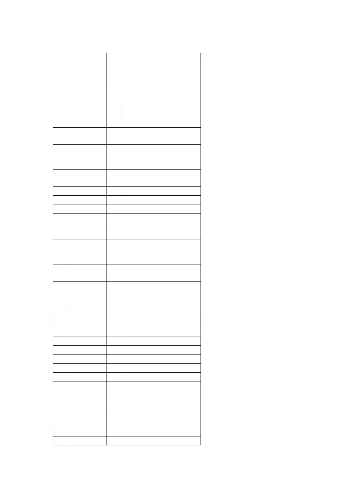
Pin
No.
Terminal
Name
I/O Function
47 GIO8 O SC DSC25 communication
data bus (DSP_BFSR1:
receiving frame)
48 GIO7 O SC DSC25 communication
data bus (it is 'L' at the
time of SD load
discontinuation)
49 GIO6 O SC DSC25 communication
data bus (’L’:Reading)
50 GIO5 O SC DSC25 communication
data bus ('L' when a
shutter may be shut)
51 GIO4 O MAIN DSC25
communication data bus
52 GIO3 O MN5772 IRQ3
53 GIO2 O MN5772 IRQ2
54 GIO1 O MN5772 IRQ
55 GIO0 O DSKDET (’H’: Loading/
ejecting)
56 CVDD2 P Power supply
57 RESET I Reset signal input (It is 'L'
at the time not more than
VCC=2.9V)
58 PWDWN I Power down signal input (’
L’)
59 CGND2 P DE
60 TCK I For JTAG
61 TDI I For JTAG
62 TMS I For JTAG
63 TRST I For JTAG
64 TEST0 I DSC25 test mode 0 (’L’)
65 TEST1 I DSC25 test mode 1 (’L’)
66 TEST2 I MXI clock selection (’L’)
67 TEST3 I (’L’)
68 TEST4 I (’H’)
69 TEST5 I (’L’)
70 TEST6 I (’L’)
71 SCANEN I Not used. (’L’)
72 TDO O For JTAG
73 USB_DP - Not used. (Open)
74 USB_DM - Not used. (Open)
75 USB_V
DD
P USB power supply
76 PLLV
DD
1 P Power supply
60